Hardware
The AS5047U's pins, bus settings, frames, timing, power and magnet, as the driver uses them.
Datasheet sections this page relies on
From ams OSRAM DS000637 v1-01:
- Pins and package: Pin Assignment, p. 3
- Supply voltage, 3.3 V and 5 V operation: Electrical Characteristics; Power Management, p. 6
- Power-up time and SPI timing: Timing Characteristics; SPI Timing, p. 9
- SPI mode, frames and the read pipeline: SPI Interface (Slave); SPI Transaction, p. 16
- Pad byte of 32-bit frames: PAD Word, p. 22
- CRC-8 of a frame: CRC Checksum, p. 23
- Reference circuit: Circuit Diagram, p. 44
- Package and magnet placement: Package Drawings & Markings; Mechanical Data, p. 45
All of them, with the driver API for each: Datasheet map.
Every value on this page comes from the AS5047U datasheet (ams OSRAM DS000637, v1-01); figure numbers refer to it. The driver is not verified on hardware yet: the values are the datasheet's, and the driver's behaviour against them is tested on the register model only.
Pins
TSSOP-14 (Figures 3 and 4). Directions are seen from the chip. The pinout, the block diagram, the circuits and the
tables on this page are drawn from docs/hardware.yml.
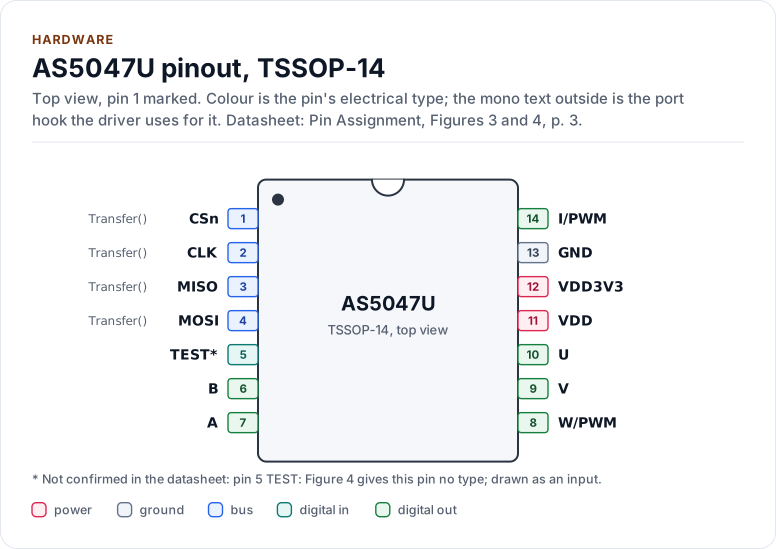
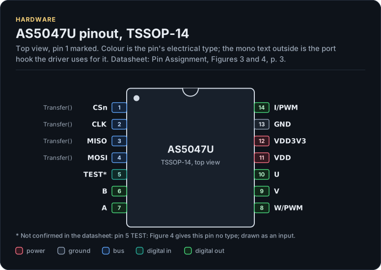
Figure description and sources
The AS5047U seen from the top, in its TSSOP-14 package. Pin 1 is marked by the dot; the numbers run counter-clockwise from it. Each pad is coloured by the pin's electrical type (legend below). Next to it is the pin's name and, in mono, the hook of the driver's port that drives or reads it; a pin without a hook is not used by the driver.
Drawn from: docs/hardware.yml; inc/as5047u_spi_interface.hpp.
TSSOP-14, 14 pins (Pin Assignment, Figures 3 and 4, p. 3).
| Pin | Name | Type (domain) | Function | Driver hook | If unused | Datasheet |
|---|---|---|---|---|---|---|
| 1 | CSn |
bus (VDD) | SPI chip select, active low | Transfer() |
Pull up | Pin Assignment, Figures 3 and 4, p. 3 |
| 2 | CLK |
bus (VDD) | SPI clock, up to 10 MHz, mode 1 | Transfer() |
Pull down | SPI Interface (Slave), p. 16 |
| 3 | MISO |
bus (VDD) | SPI data out | Transfer() |
Leave open | Pin Assignment, Figures 3 and 4, p. 3 |
| 4 | MOSI |
bus (VDD) | SPI data in | Transfer() |
Pull down | Pin Assignment, Figures 3 and 4, p. 3 |
| 5 | TEST 1 |
digital in (VDD) | Test pin; connect to ground | - | Connect to GND | Pin Assignment, Figures 3 and 4, p. 3 |
| 6 | B |
digital out (VDD) | Incremental signal B | - | Leave open | Pin Assignment, Figures 3 and 4, p. 3 |
| 7 | A |
digital out (VDD) | Incremental signal A | - | Leave open | Pin Assignment, Figures 3 and 4, p. 3 |
| 8 | W/PWM |
digital out (VDD) | Commutation signal W, or the PWM output | - | Leave open | Pin Assignment, Figures 3 and 4, p. 3 |
| 9 | V |
digital out (VDD) | Commutation signal V | - | Leave open | Pin Assignment, Figures 3 and 4, p. 3 |
| 10 | U |
digital out (VDD) | Commutation signal U | - | Leave open | Pin Assignment, Figures 3 and 4, p. 3 |
| 11 | VDD |
power (VDD) | Supply: 4.5 V to 5.5 V into the on-chip LDO, or 3.0 V to 3.6 V tied to VDD3V3 | - | - | Electrical Characteristics, Figure 6, p. 6 |
| 12 | VDD3V3 |
power (VDD) | 3.3 V LDO output with 1 µF to GND; in 3.3 V operation tied to VDD | - | - | Pin Assignment, Figure 4, p. 4 |
| 13 | GND |
ground | Ground | - | - | Pin Assignment, Figure 4, p. 4 |
| 14 | I/PWM |
digital out (VDD) | Index signal I, or the PWM output | - | Leave open | Pin Assignment, Figure 4, p. 4 |
Source of this table and of the chip figures: docs/hardware.yml.
The chip has no reset pin and no interrupt pin, so the port has no GPIO hook. Digital inputs must never float. The ABI, UVW and PWM outputs drive at most 4 mA at 5 V and 2 mA at 3.3 V, into at most 50 pF.
Inside the chip
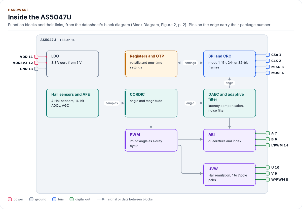
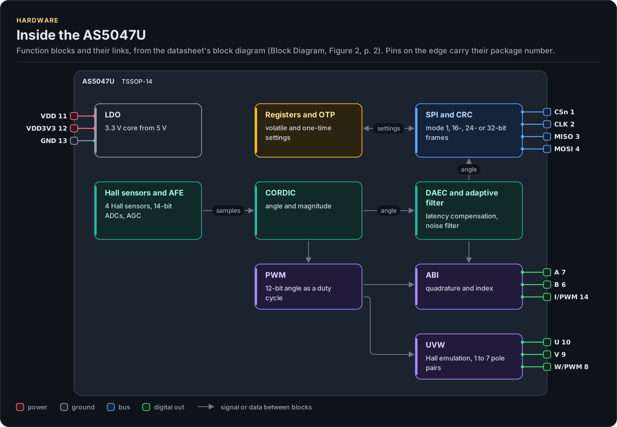
Figure description and sources
The AS5047U's function blocks inside its outline. Arrows between blocks carry signals or data in the direction they point (both ways where they have two heads). The package pins stand on the left and right edges with their numbers, each wired to the block it reaches.
Drawn from: docs/hardware.yml; inc/as5047u_spi_interface.hpp.
Circuits
The minimum circuit of Figure 61, with the 5 V supply: the on-chip LDO makes VDD3V3, which needs its own 1 µF and powers nothing else. The ABI, UVW and PWM outputs are left open, as Figure 4 allows.
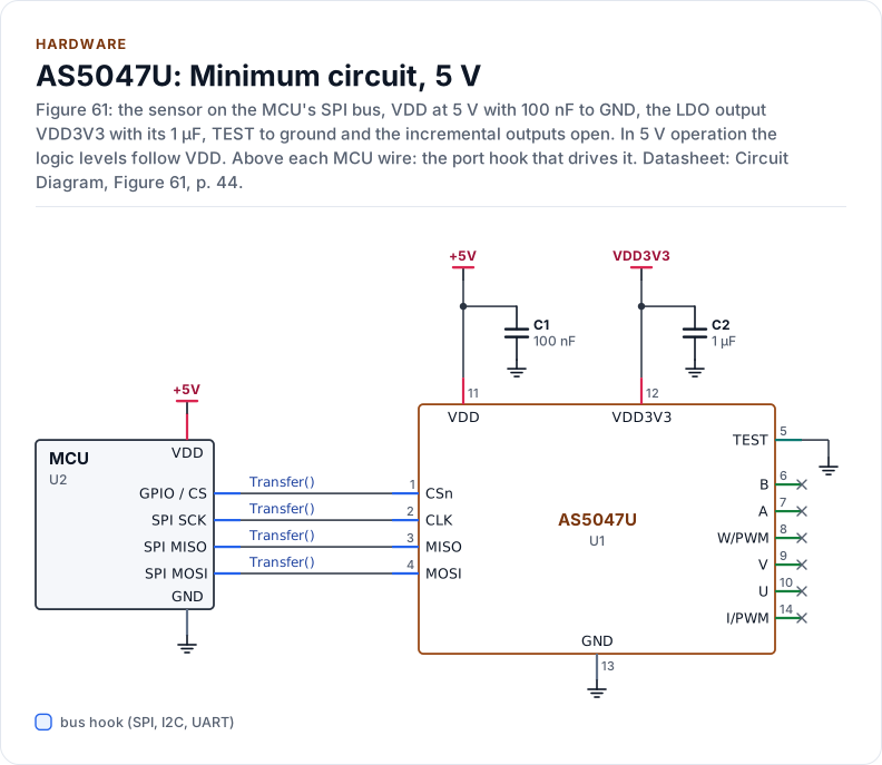
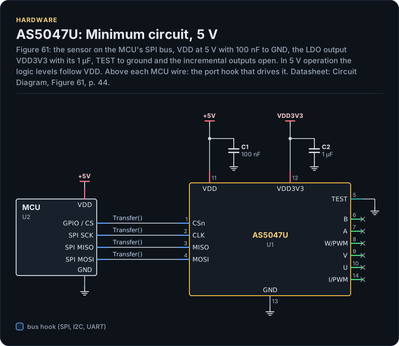
Figure description and sources
A schematic. The MCU is on the left, each of its pins level with the chip pin it connects to; above each wire is the hook of the driver's port that drives or reads it. Supply pins point up to their supply and decoupling, ground pins down. Pins on the right carry the loads and the pins tied to a supply or ground; a cross marks a pin left open. A dot is a junction; wires that cross without a dot are not connected.
Drawn from: docs/hardware.yml; inc/as5047u_spi_interface.hpp.
With a 3.3 V supply, VDD and VDD3V3 are tied together (Figure 11), and the logic levels match a 3.3 V MCU without a level shifter.
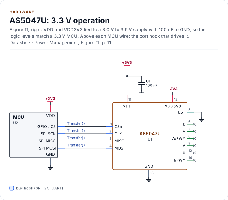
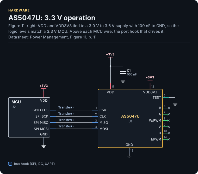
Figure description and sources
A schematic. The MCU is on the left, each of its pins level with the chip pin it connects to; above each wire is the hook of the driver's port that drives or reads it. Supply pins point up to their supply and decoupling, ground pins down. Pins on the right carry the loads and the pins tied to a supply or ground; a cross marks a pin left open. A dot is a junction; wires that cross without a dot are not connected.
Drawn from: docs/hardware.yml; inc/as5047u_spi_interface.hpp.
Minimum circuit, 5 V (figure chip-circuit-typical)
| Part | Kind | Value | Connects | Datasheet |
|---|---|---|---|---|
| U2 | MCU | - | VDD: +5V, GND: GND, SCK: CLK, MOSI: MOSI, MISO: MISO, CS: CSn | Circuit Diagram, Figure 61, p. 44 |
| C1 | capacitor | 100 nF | +5V, GND | Circuit Diagram, Figure 61, p. 44 |
| C2 | capacitor | 1 µF | VDD3V3, GND | Circuit Diagram, Figure 61, p. 44 |
3.3 V operation (figure chip-circuit-supply-3v3)
| Part | Kind | Value | Connects | Datasheet |
|---|---|---|---|---|
| U2 | MCU | - | VDD: +3V3, GND: GND, SCK: CLK, MOSI: MOSI, MISO: MISO, CS: CSn | Power Management, Figure 11, p. 11 |
| C1 | capacitor | 100 nF | +3V3, GND | Power Management, Figure 11, p. 11 |
Export a circuit for a schematic or PCB tool: kokeb-docs hardware --kicad-netlist OUT.net --circuit typical.
Bus settings
| Setting | Value |
|---|---|
| SPI mode | 1: CPOL = 0, CPHA = 1. The chip samples MOSI on the falling edge of CLK. Modes 0, 2 and 3 do not work |
| Clock | Up to 10 MHz (t_clk ≥ 100 ns) |
| Bit order | MSB first |
| Chip select | Active low, one frame per low period. CSn must go high between frames: the chip finds the frame length from the CSn low time and executes the frame on the rising edge |
| Reply | The reply to a frame arrives during the next frame |
| Driver default | 24-bit frames with CRC-8 (FrameFormat::Bits24) |
Frames
"SPI Transaction" section, Figures 20 to 28. RW is 1 for a read and 0 for a write.
| Format | MOSI (host to chip) | MISO (chip to host) | Driver |
|---|---|---|---|
| 16 bit | [14] RW = 1, [13:0] address |
[15] warning, [14] error, [13:0] data |
Bits16: reads only, no CRC |
| 24 bit | [22] RW, [21:8] address or data, [7:0] CRC |
[23] warning, [22] error, [21:8] data, [7:0] CRC |
Bits24: the default |
| 32 bit | [31:24] pad, then the 24-bit frame |
The 24-bit frame, then [7:0] pad |
Bits32: daisy chains, pad from Config::pad_byte |
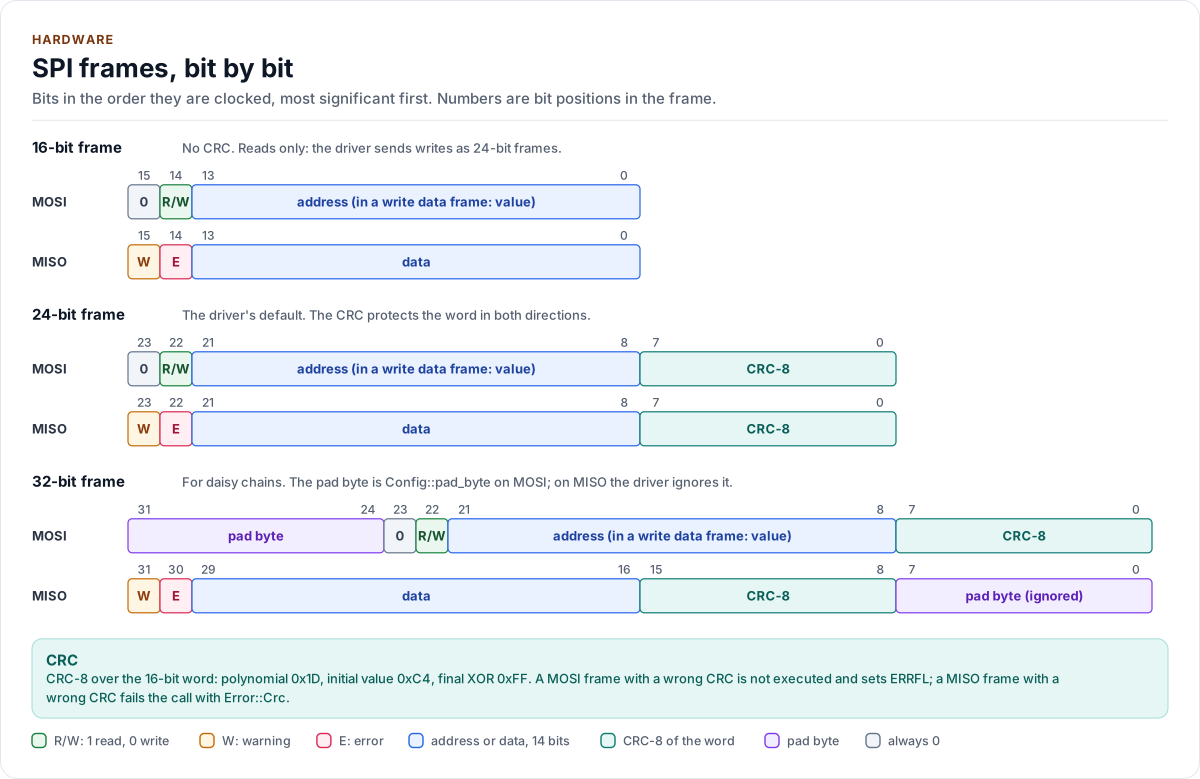
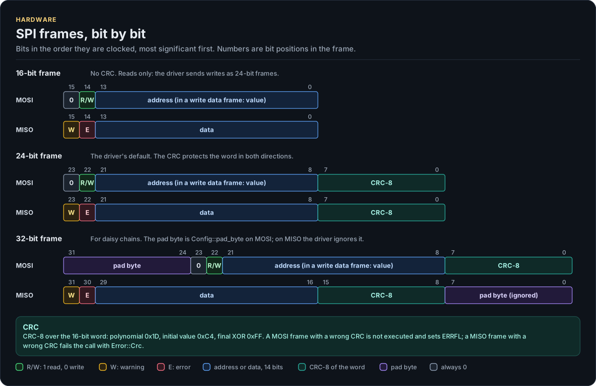
Figure description and sources
Each frame is drawn in the order it is clocked, most significant bit first, and the numbers above a row are bit positions in that frame. On MOSI the 16-bit command word holds the R/W bit (1 to read, 0 to write) and a 14-bit address; the data frame of a write has the same layout with R/W at 0 and the 14-bit value in place of the address. On MISO the reply word holds the warning bit, the error bit (a flag is set in ERRFL) and 14 data bits. The 24-bit frame adds the CRC-8 of the word in both directions. The 32-bit frame adds the pad byte: first on MOSI (the driver sends Config::pad_byte), last on MISO (the driver ignores it). The bit positions come from the frame constants in inc/as5047u_registers.hpp and the byte order from detail::FrameBus::Exchange in inc/as5047u_spi_interface.hpp. With 16-bit frames the driver sends writes as 24-bit frames.
Drawn from: inc/as5047u_registers.hpp frame bits; inc/as5047u_spi_interface.hpp detail::FrameBus::Exchange; inc/as5047u_spi_interface.hpp Crc8; inc/as5047u.hpp writeFormat; figure module docs/diagrams/figures/spi-frames.py.
The datasheet allows 16-bit frames for reads only, so with Bits16 the driver sends every write as a 24-bit
frame. Writes are always CRC-protected, and ProgramOtp() sends every frame, reads included, as a 24-bit frame
whatever Config::frame says, then restores the format.
The CRC is CRC-8 with polynomial 0x1D, initial value 0xC4 and final XOR 0xFF, over the 16-bit word ("CRC
Checksum"); as5047u::Crc8() computes it. A MOSI frame with a wrong CRC is not executed and sets ERRFL.CRC_error.
A MISO frame with a wrong CRC fails the call with Error::Crc.
Read and write sequences
A read is two frames: the read command, then a NOP whose reply carries the data. When the reply's error bit is set, the driver reads ERRFL (two more frames, and the read clears it on the chip) to find out why.
sequenceDiagram
    participant D as Driver
    participant C as AS5047U
    D->>C: read ANGLECOM (0x3FFF)
    C-->>D: reply to the previous frame (discarded)
    D->>C: read NOP (0x4000)
    C-->>D: ANGLECOM data, warning and error bits, CRC
    Note over D: error bit set? read ERRFL and fail the call
A write is two frames, the command (RW = 0, address) and the data. The reply to the data frame reports on the
command frame. With Verify::ReadBack, and always in EnsureInitialized() and ProgramOtp(), each write is then
read back (two more frames) and compared. Brackets give the count with Verify::ReadBack.
| Call | Frames | Clock time, 24-bit frames at 10 MHz |
|---|---|---|
ReadAngleCounts() and every other single read, reply with no flag bit |
2 | 4.8 µs |
| The same with a flagged reply (ERRFL read) | 4 | 9.6 µs |
WriteRegister() |
2 [4] | 4.8 µs [9.6 µs] |
ReadNonVolatile() |
14 | 33.6 µs |
ApplyConfig(), SetZeroPosition(), SetDirection() |
26 [38] | 62.4 µs [91.2 µs] |
EnsureInitialized(), chip already up |
44 (20 with write_settings = false) |
105.6 µs (48 µs) |
EnsureInitialized(), chip not yet ready |
2 more per poll, 1 ms apart, up to startup_timeout_ms |
|
SetZeroHere() |
54 [78] | 129.6 µs [187.2 µs] |
ProgramOtp() |
100 at least, plus 2 per millisecond of burn time | 240 µs plus the burn |
The times are derived (3 bytes of clock per frame), not measured. Add at least 350 ns of CSn high time per frame and your port's own overhead. A reply with the error bit set adds 2 frames for ERRFL.
Timing
Figure 19. The two 350 ns limits are the ones a port can break: CSn low to the first clock edge, and CSn high between two frames. A hardware chip select usually meets them; a GPIO chip select toggled right next to the transfer may not.
| Symbol | Parameter | Min | Max | Unit |
|---|---|---|---|---|
| t_L | CSn falling edge to first CLK rising edge | 350 | ns | |
| t_clk | Clock period | 100 | ns | |
| t_clkH, t_clkL | Clock high and low time | 50 | ns | |
| t_H | Last CLK falling edge to CSn rising edge | t_clk / 2 | ns | |
| t_CSn | CSn high time between frames | 350 | ns | |
| t_MOSI | MOSI valid before the clock edge | 20 | ns | |
| t_MISO | Clock edge to MISO valid | 51 | ns | |
| t_OZ | CSn rising edge to MISO high impedance | 10 | ns | |
| t_pon | VDD above its minimum to the first valid angle | 10 | ms |
EnsureInitialized() covers t_pon itself: it polls DIA once per millisecond until every loop reports finished, for
at most Config::startup_timeout_ms (default 10 ms, t_pon). The deadline counts from the first poll, so raise it if
your supply ramps slowly or the start comes before VDD is up. The only other wait is in ProgramOtp(), 1 ms between
polls of the burn. Both go through the port's DelayUs().
Power
| Mode | Supply pins | Temperature | Angle noise (rms) |
|---|---|---|---|
| 5 V | VDD 4.5 V to 5.5 V; VDD3V3 is the LDO output, 1 µF to GND | -40 °C to 150 °C | 0.068° |
| 3.3 V, NOISESET = 0 | VDD and VDD3V3 tied, 3.0 V to 3.6 V | -40 °C to 125 °C | 0.068° |
| 3.3 V, NOISESET = 1 | VDD and VDD3V3 tied, 3.0 V to 3.6 V | -40 °C to 150 °C | 0.082° |
Config::high_temperature_noisesets NOISESET, for 150 °C operation at 3.3 V.- Supply current is at most 16 mA. Put 100 nF from VDD to GND in both modes.
- Logic levels follow VDD: V_IH ≥ 0.7 × VDD, V_IL ≤ 0.3 × VDD. In 5 V mode a 3.3 V MCU needs a level shifter on CLK, MOSI and CSn (0.7 × 4.5 V = 3.15 V), and MISO swings up to VDD.
- Absolute maximum: 7.0 V on VDD, 5.0 V on VDD3V3.
- The chip has no low-power mode:
Deinitialize()does no I/O. ReadDiagnostics().value.vdd_5vis true in 5 V mode.- Burning the OTP has its own supply and temperature limits: OTP programming.
Magnet
| Parameter | Value |
|---|---|
| Type | Diametrically magnetised (two poles across the diameter), centred on the package axis |
| Field at the die | 35 mT to 70 mT, orthogonal component, along a circle of 1.1 mm radius |
| Datasheet reference magnet | N35H, 8 mm diameter, 3 mm thick |
| Speed | Up to 28000 rpm |
| Accuracy (optimal placement) | ±0.8° at 25 °C, ±1° over -40 °C to 150 °C (maximum non-linearity) |
The AGC keeps the field magnitude constant while the field is in range. ReadAgc() near 0 means the field is too
strong (magnet too close), near 255 too weak (too far); ERRFL.AGC_warning is set at either limit. Read ERRFL or AGC
regularly: the datasheet requires one of them to be read for the AGC loop to work as specified.
Outputs other than SPI
| Output | Pins | What it carries | Config fields |
|---|---|---|---|
| ABI | A, B, I/PWM | Quadrature, 25 to 4096 pulses per revolution; index once per revolution, 3 LSB or 1 LSB wide | incremental, abi_enable, abi_resolution_code, abi_decimal, index_width, hysteresis_code |
| UVW | U, V, W/PWM | Hall-sensor emulation for 1 to 7 pole pairs | incremental, uvw_enable, uvw_pole_pairs |
| PWM | W/PWM or I/PWM | 12-bit angle in a frame of 4119 PWM clocks of 444 ns typical (about 1.83 ms) | pwm_enable |
The PWM goes on pin W when ABI is selected and on pin I when UVW is selected (SETTINGS2.UVW_ABI).
Config::uncompensated_at_angle_register (SETTINGS2.Data_select) makes address 0x3FFF and the PWM output carry the
angle without DAEC. Configuration maps each field to its register.
Reference documents
| Document | Revision | Get it |
|---|---|---|
| Datasheet: AS5047U High Resolution Rotary Position Sensor (ams OSRAM DS000637) | v1-01, 2020-12-16 | vendor page |
Written against these revisions; the SHA-256 of each file is in docs/datasheets.yml. Where each part
of the driver is in the datasheet: Datasheet map.
| Also useful | Contents |
|---|---|
| Application note AS5x47U Adaptive Filter (ams OSRAM, from the same vendor page) | Choosing K_min and K_max for the velocity filter |
inc/as5047u_registers.hpp |
The register map as the driver uses it, with datasheet figure numbers |
-
Not confirmed in the datasheet: pin 5 (TEST): Figure 4 gives this pin no type; drawn as an input. ↩