Figures
Every figure on this site is drawn by a Python module from facts extracted from the code, so it is rebuilt,
not redrawn, when the code changes. CI runs kokeb-docs figures --check and fails when a
committed figure no longer matches the code. Each figure below lists the files it is drawn from.
Inside the PF1550
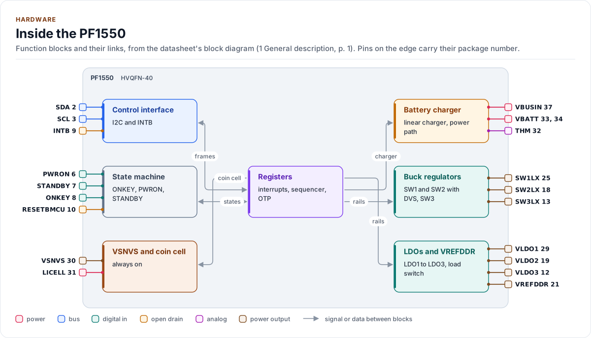
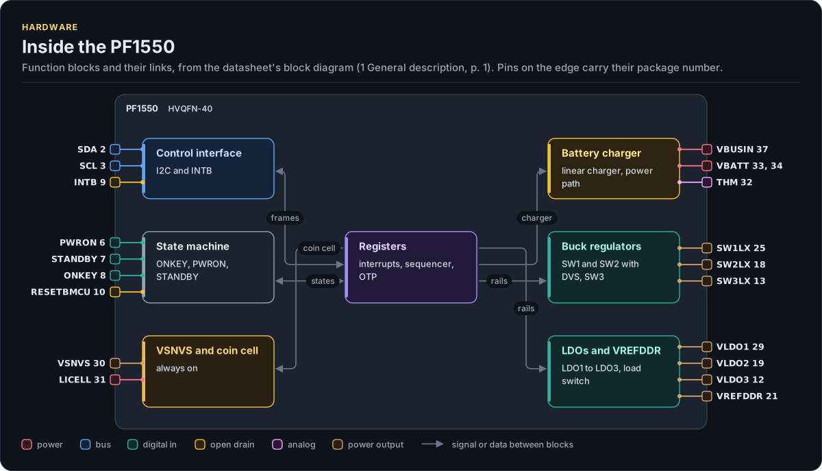
Figure description and sources
The PF1550's function blocks inside its outline. Arrows between blocks carry signals or data in the direction they point (both ways where they have two heads). The package pins stand on the left and right edges with their numbers, each wired to the block it reaches.
Drawn from: docs/hardware.yml; inc/pf1550_i2c_interface.hpp.
Hardware description: docs/hardware.yml
Drawn from:
PF1550: Control connections to a host processor
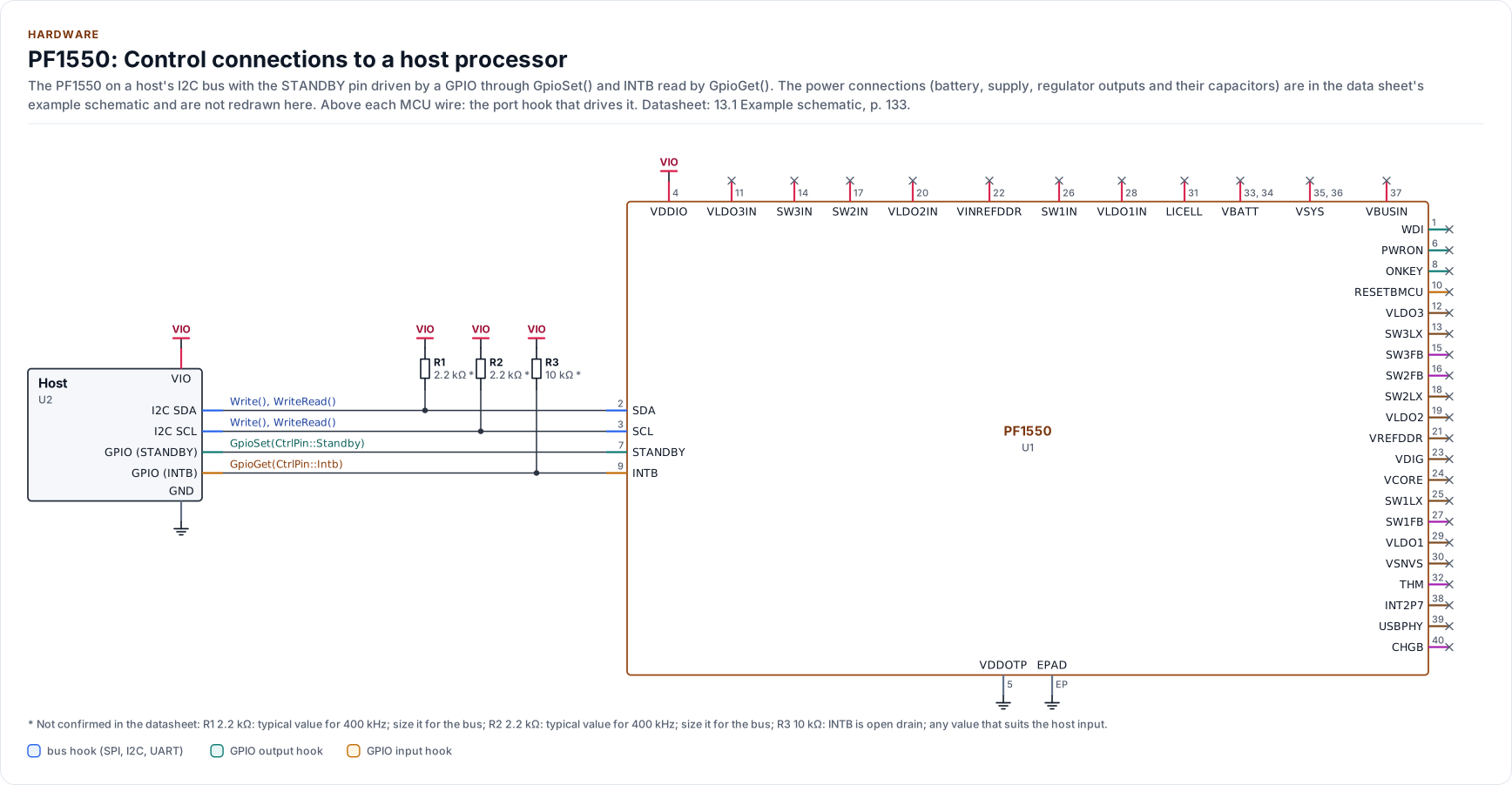
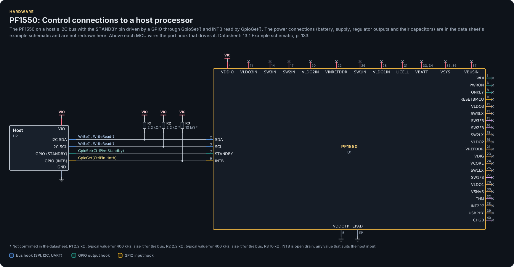
Figure description and sources
A schematic. The MCU is on the left, each of its pins level with the chip pin it connects to; above each wire is the hook of the driver's port that drives or reads it. Supply pins point up to their supply and decoupling, ground pins down. Pins on the right carry the loads and the pins tied to a supply or ground; a cross marks a pin left open. A dot is a junction; wires that cross without a dot are not connected.
Drawn from: docs/hardware.yml; inc/pf1550_i2c_interface.hpp.
Hardware description: docs/hardware.yml
Drawn from:
PF1550 package, HVQFN-40
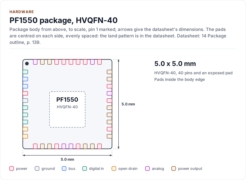
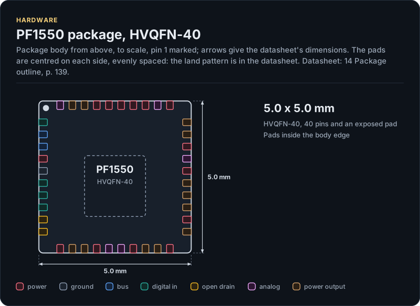
Figure description and sources
The PF1550 package seen from the top and, when the height is known, from the side, drawn to scale: 5.0 x 5.0 mm. The arrows carry the datasheet's dimensions, the dot marks pin 1 and the pads are numbered counter-clockwise from it, coloured by the pin's electrical type (legend below). Pads sit centred on each side, evenly spaced; the datasheet's land pattern is the reference for a board.
Drawn from: docs/hardware.yml; inc/pf1550_i2c_interface.hpp.
Hardware description: docs/hardware.yml
Drawn from:
PF1550 pinout, HVQFN-40
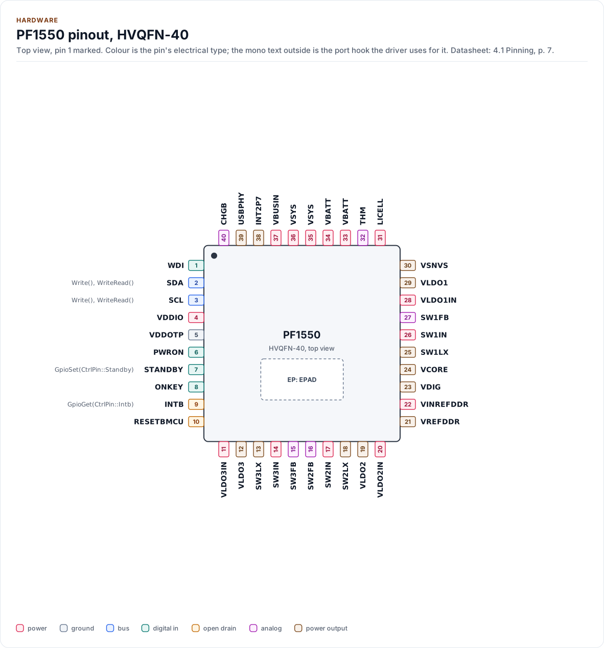
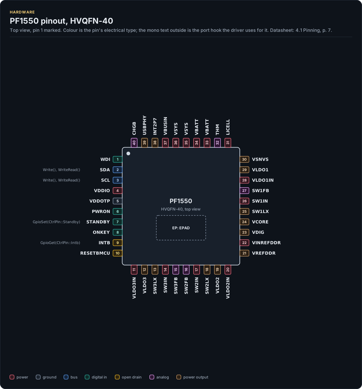
Figure description and sources
The PF1550 seen from the top, in its HVQFN-40 package. Pin 1 is marked by the dot; the numbers run counter-clockwise from it. Each pad is coloured by the pin's electrical type (legend below). Next to it is the pin's name and, in mono, the hook of the driver's port that drives or reads it; a pin without a hook is not used by the driver. The dashed square is the exposed pad.
Drawn from: docs/hardware.yml; inc/pf1550_i2c_interface.hpp.
Hardware description: docs/hardware.yml
Drawn from:
The layers, one of them yours
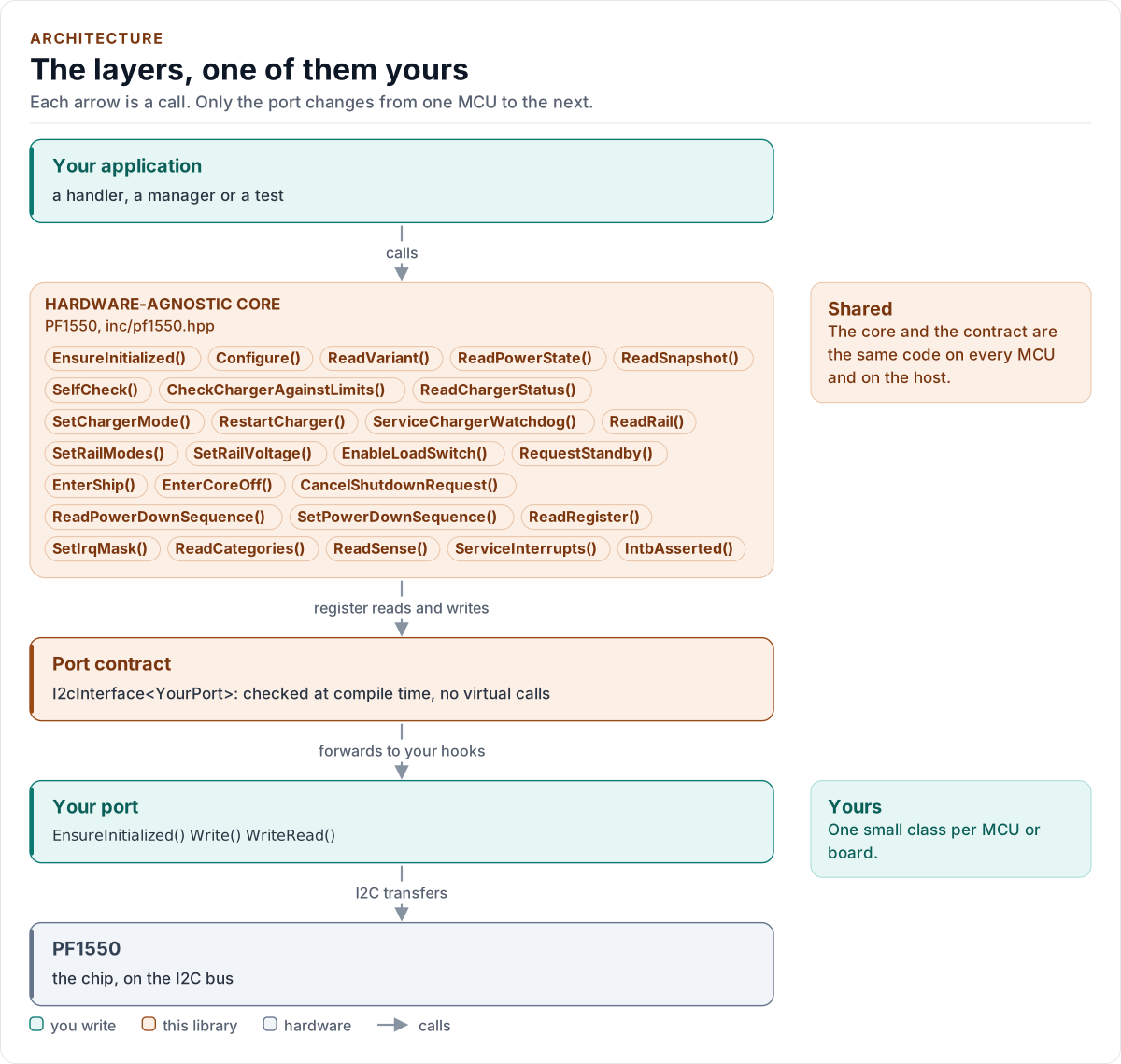
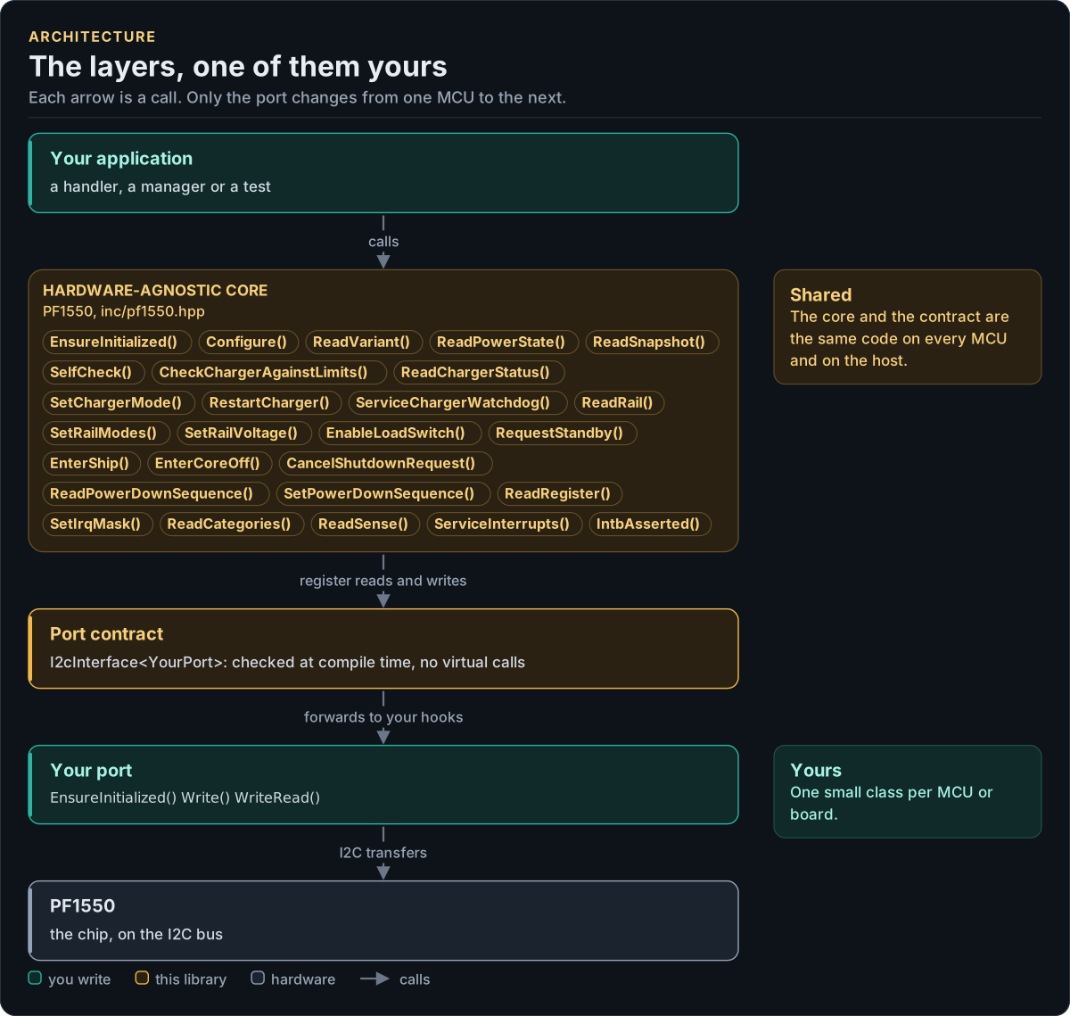
Figure description and sources
Top to bottom, each arrow is a call. Your application calls one object, whose public calls are listed from the umbrella header in inc/. The core turns each call into register reads and writes and hands them to the port contract (the CRTP base in inc/*_interface.hpp), which forwards them, at compile time, to the hooks of the port class you write; your port moves the bytes on the bus. The notes on the right say which layers stay the same on every MCU and which one you write. A library without a port contract has only the first two layers.
Drawn from: inc/pf1550.hpp public calls; inc/pf1550_i2c_interface.hpp I2cInterface; figure module docs/diagrams/figures/driver-layers.py.
Figure module: docs/diagrams/figures/driver-layers.py
Drawn from:
public callsininc/pf1550.hppI2cInterfaceininc/pf1550_i2c_interface.hpp
One register read on the I2C bus
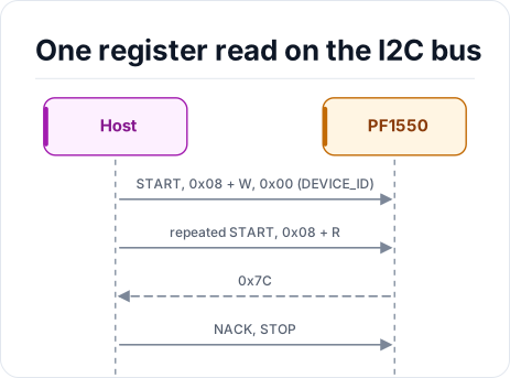
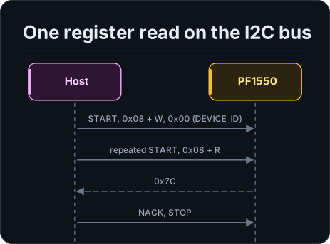
Figure description and sources
Participants, left to right: Host and PF1550. The steps run from top to bottom. Host sends START, 0x08 + W, 0x00 (DEVICE_ID) to PF1550. Host sends repeated START, 0x08 + R to PF1550. PF1550 returns 0x7C to Host. Host sends NACK, STOP to PF1550.
Drawn from: docs/model/i2c-register-read.seq.yml.
Hardware description: docs/model/i2c-register-read.seq.yml
Drawn from:
One call through the layers
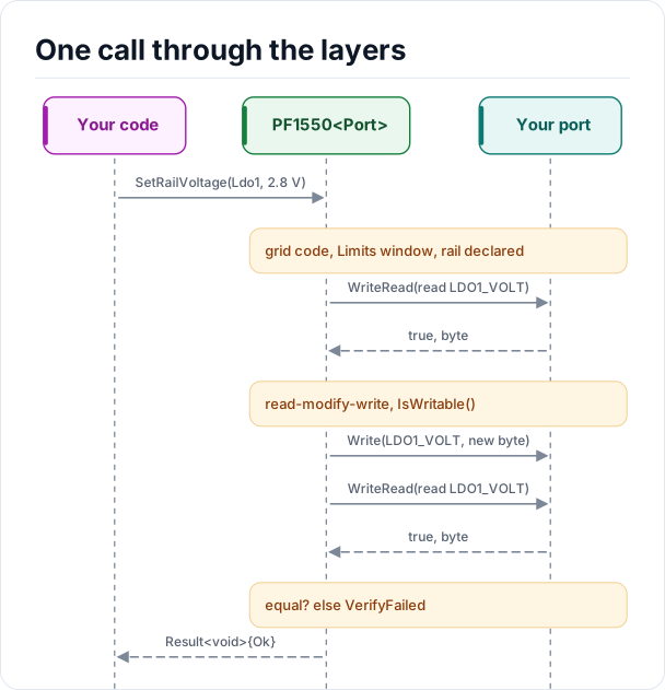
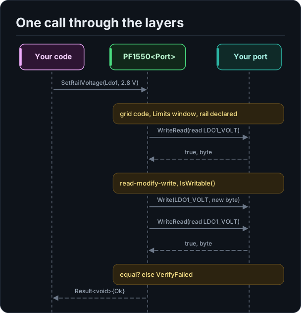
Figure description and sources
Participants, left to right: Your code, PF1550
Drawn from: docs/model/one-call-through-the-layers.seq.yml.
Hardware description: docs/model/one-call-through-the-layers.seq.yml
Drawn from: