Hardware
The PF1550's package, pins, bus settings and power, as the driver uses them. The driver reaches the chip through the I2C bus and two optional pins, STANDBY and INTB; everything else on the package is wired by the board, as the datasheet's example schematic shows (section 13.1, p. 133).
Datasheet sections this page relies on
From NXP Semiconductors PF1550 7:
- Pins and package: 4.2 Pin definitions, p. 8
- I2C address, clock and register framing: 9.7 Control interface I2C block description, p. 71
- Example schematic: 13.1 Example schematic, p. 133
- Package outline: 14 Package outline, p. 139
All of them, with the driver API for each: Datasheet map.
Package
HVQFN-40, 5.0 mm x 5.0 mm with an exposed pad (data sheet section 14, p. 139). The exposed pad is ground. The body size is the only dimension the datasheet text gives; the pitch and the height are on its drawing and are not drawn here.
Pins
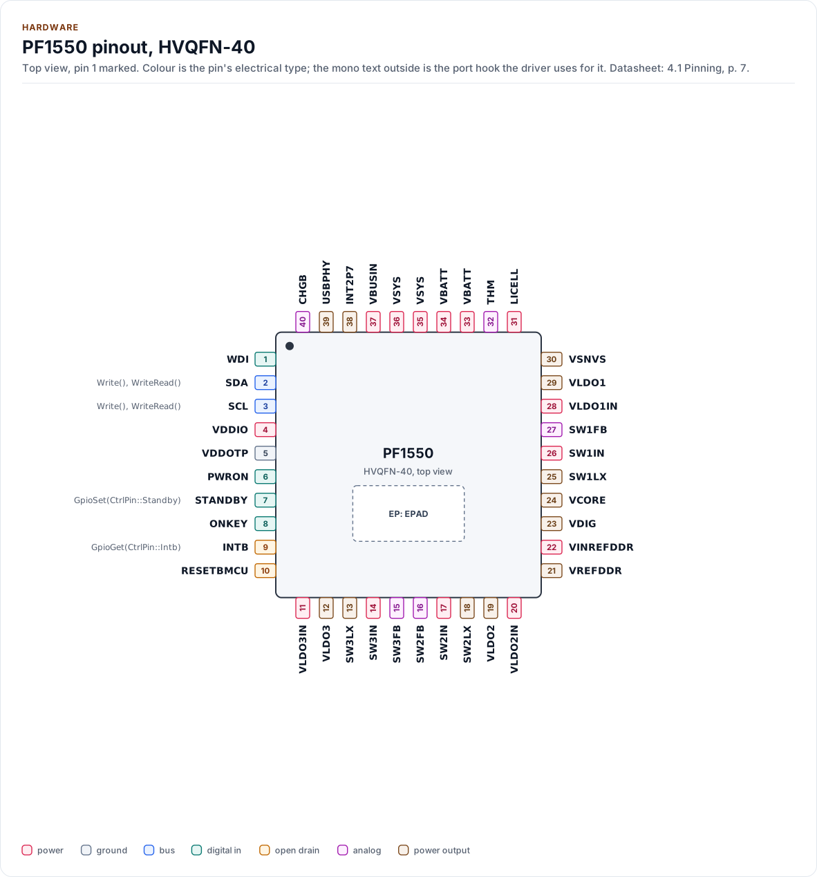
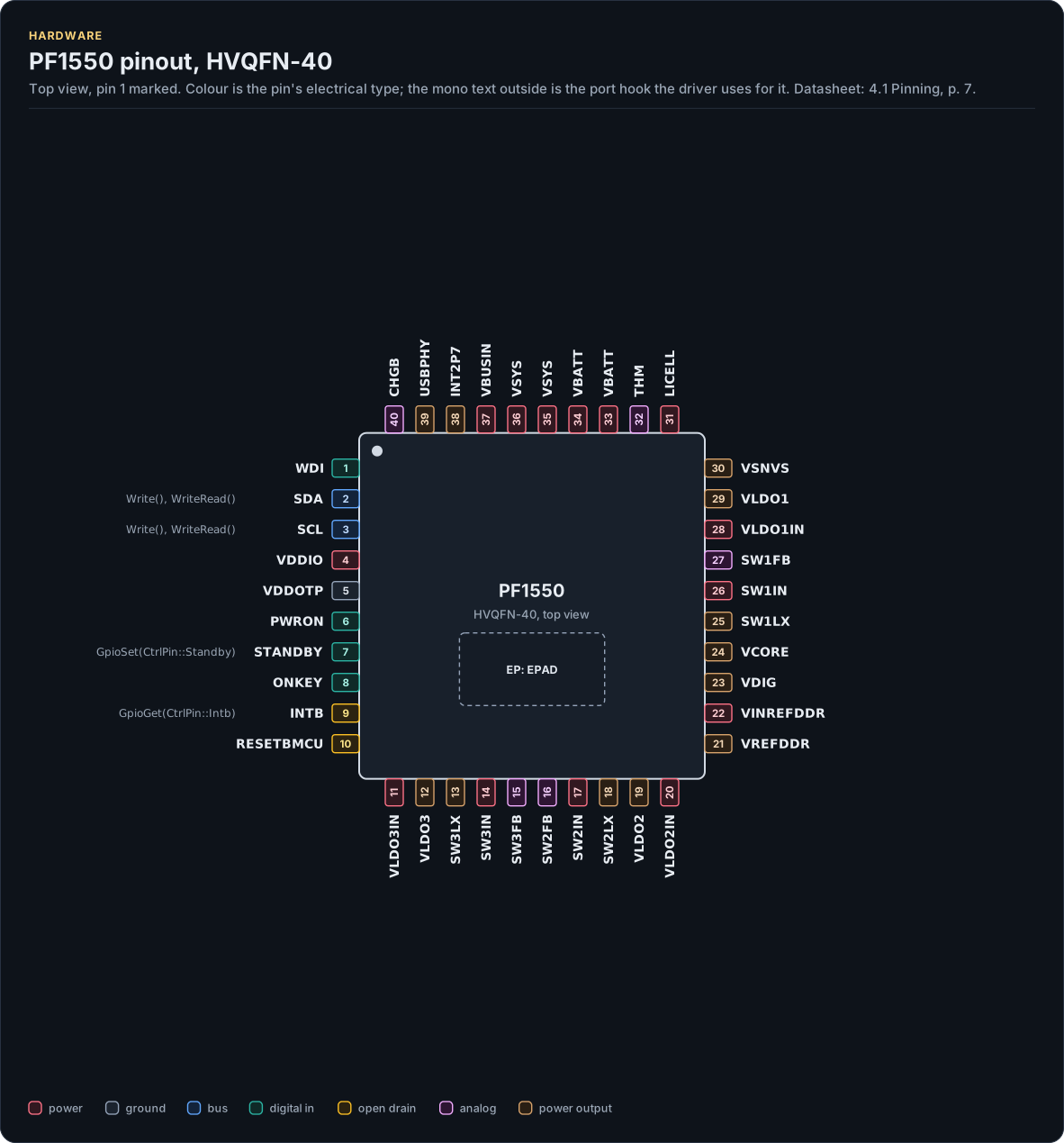
Figure description and sources
The PF1550 seen from the top, in its HVQFN-40 package. Pin 1 is marked by the dot; the numbers run counter-clockwise from it. Each pad is coloured by the pin's electrical type (legend below). Next to it is the pin's name and, in mono, the hook of the driver's port that drives or reads it; a pin without a hook is not used by the driver. The dashed square is the exposed pad.
Drawn from: docs/hardware.yml; inc/pf1550_i2c_interface.hpp.
HVQFN-40, 40 pins and an exposed pad (4.1 Pinning, p. 7).
| Pin | Name | Type (domain) | Function | Driver hook | If unused | Datasheet |
|---|---|---|---|---|---|---|
| 1 | WDI |
digital in (VDDIO) | Watchdog input from the processor | - | - | 4.2, p. 8 |
| 2 | SDA |
bus (VDDIO) | I2C data | Write(), WriteRead() |
- | 9.7, p. 71 |
| 3 | SCL |
bus (VDDIO) | I2C clock, up to 400 kHz | Write(), WriteRead() |
- | 9.7, p. 71 |
| 4 | VDDIO |
power (VDDIO) | I/O supply, 1.7 V to 3.3 V | - | - | 4.2, p. 8 |
| 5 | VDDOTP |
ground | Connect to ground in the application | - | - | 4.2, p. 8 |
| 6 | PWRON |
digital in (VDDIO) | PWRON input | - | - | 9.1, p. 68 |
| 7 | STANDBY |
digital in (VDDIO) | STANDBY input; the driver drives it | GpioSet(CtrlPin::Standby) |
Leave low (STANDBYINV = 0) | 9.2, p. 69 |
| 8 | ONKEY |
digital in (VDDIO) | ONKEY push-button input | - | - | 9.6, p. 71 |
| 9 | INTB |
open drain (VDDIO) | Interrupt output, active low | GpioGet(CtrlPin::Intb) |
Leave open; poll with ServiceInterrupts() | 9.4, p. 70 |
| 10 | RESETBMCU |
open drain (VDDIO) | Reset output to the processor | - | - | 9.3, p. 69 |
| 11 | VLDO3IN |
power (VSYS) | LDO3 input supply | - | - | 7, p. 34 |
| 12 | VLDO3 |
power output (VLDO3) | LDO3 output | - | - | 7, p. 34 |
| 13 | SW3LX |
power output (SW3) | Buck 3 switching node | - | - | 6, p. 24 |
| 14 | SW3IN |
power (VSYS) | Buck 3 input supply | - | - | 6, p. 24 |
| 15 | SW3FB |
analog (SW3) | Buck 3 output voltage feedback | - | - | 6, p. 24 |
| 16 | SW2FB |
analog (SW2) | Buck 2 output voltage feedback | - | - | 6, p. 24 |
| 17 | SW2IN |
power (VSYS) | Buck 2 input supply | - | - | 6, p. 24 |
| 18 | SW2LX |
power output (SW2) | Buck 2 switching node | - | - | 6, p. 24 |
| 19 | VLDO2 |
power output (VLDO2) | LDO2 output | - | - | 7, p. 34 |
| 20 | VLDO2IN |
power (VSYS) | LDO2 input supply | - | - | 7, p. 34 |
| 21 | VREFDDR |
power output (VREFDDR) | VREFDDR output | - | - | 7, p. 34 |
| 22 | VINREFDDR |
power (VSYS) | VREFDDR input supply | - | - | 7, p. 34 |
| 23 | VDIG |
power output (INT) | Digital regulator output, used inside the chip | - | - | 4.2, p. 8 |
| 24 | VCORE |
power output (INT) | Core regulator output, used inside the chip | - | - | 4.2, p. 8 |
| 25 | SW1LX |
power output (SW1) | Buck 1 switching node | - | - | 6, p. 24 |
| 26 | SW1IN |
power (VSYS) | Buck 1 input supply | - | - | 6, p. 24 |
| 27 | SW1FB |
analog (SW1) | Buck 1 feedback input | - | - | 6, p. 24 |
| 28 | VLDO1IN |
power (VSYS) | LDO1 input supply | - | - | 7, p. 34 |
| 29 | VLDO1 |
power output (VLDO1) | LDO1 output | - | - | 7, p. 34 |
| 30 | VSNVS |
power output (VSNVS) | VSNVS regulator output | - | - | 7, p. 34 |
| 31 | LICELL |
power (LICELL) | Coin cell input and charger output | - | - | 4.2, p. 8 |
| 32 | THM |
analog (INT) | Thermistor connection; connect the thermistor to ground | - | - | 4.2, p. 8 |
| 33 | VBATT |
power (VBATT) | Battery input | - | - | 4.2, p. 8 |
| 34 | VBATT |
power (VBATT) | Battery input | - | - | 4.2, p. 8 |
| 35 | VSYS |
power (VSYS) | Main input of the PMIC and output of the charger | - | - | 4.2, p. 8 |
| 36 | VSYS |
power (VSYS) | Main input of the PMIC and output of the charger | - | - | 4.2, p. 8 |
| 37 | VBUSIN |
power (VBUS) | Charger input | - | - | 4.2, p. 8 |
| 38 | INT2P7 |
power output (INT) | 2.7 V regulator output, also the thermistor bias | - | - | 4.2, p. 8 |
| 39 | USBPHY |
power output (USBPHY) | USBPHY regulator output | - | - | 4.2, p. 8 |
| 40 | CHGB |
analog (VSYS) | Charger LED connection; the LED goes from VSYS to this pin | - | - | 4.2, p. 8 |
| EP | EPAD |
ground | Exposed pad; connect to ground | - | - | 4.2, p. 8 |
Source of this table and of the chip figures: docs/hardware.yml.
The driver uses SDA and SCL through the port, STANDBY through GpioSet(CtrlPin::Standby, ...) and INTB through
GpioGet(CtrlPin::Intb, ...). It never touches the other pins: PWRON, ONKEY, WDI and RESETBMCU belong to the board
and the state machine. The driver reads their effect (state, interrupts) and configures their debounce and polarity
where the datasheet makes them registers.
Blocks
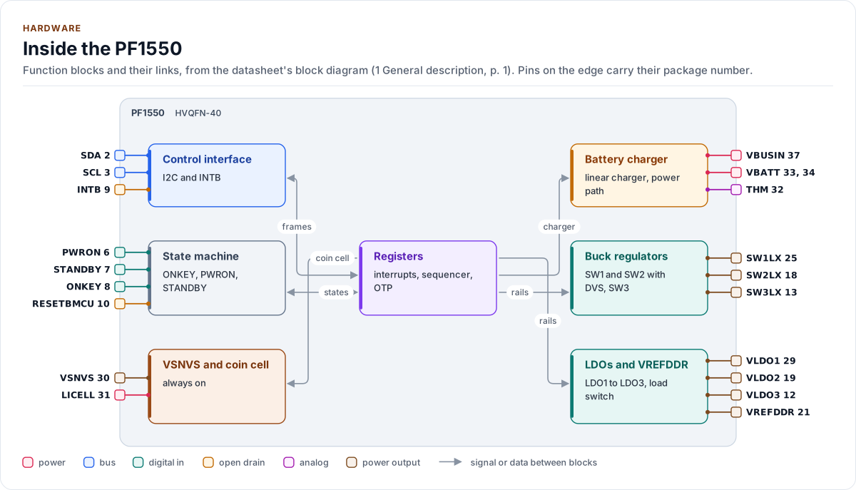
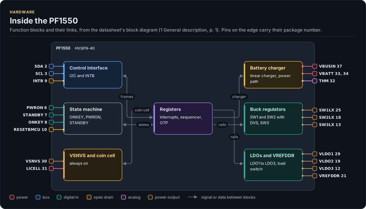
Figure description and sources
The PF1550's function blocks inside its outline. Arrows between blocks carry signals or data in the direction they point (both ways where they have two heads). The package pins stand on the left and right edges with their numbers, each wired to the block it reaches.
Drawn from: docs/hardware.yml; inc/pf1550_i2c_interface.hpp.
The register map is split in two pages by address: the PMIC registers 0x00 to 0x6F and the charger registers
0x80 to 0x9F, both on the same I2C address.
Control pins
- STANDBY is an input of the chip.
RequestStandby(true)calls yourGpioSet(CtrlPin::Standby, GpioSignal::ACTIVE);ACTIVEmeans "request STANDBY" and your port maps the polarity (STANDBYINV= 0 is active high). The driver never writesSTANDBYINVunlessPowerConfig::applyis set: change the polarity only together with the port. Without the hookRequestStandby()returnsUnsupported. - INTB is an open-drain output, low when an unmasked interrupt is pending. With
GpioGet(),ServiceInterrupts()returns an empty result without bus traffic while INTB is high. Without it, every call readsINT_CATEGORY. - PWRON, ONKEY, WDI, RESETBMCU are not driver pins. PWRON level or edge sensitivity is an OTP option
(
OTP_PWRON_CFG, option A8 is edge sensitive) and the driver cannot read it.
Bus settings
| Setting | Value |
|---|---|
| Clock | Up to 400 kHz (kMaxClockHz), fast mode |
| Address | 7-bit, 0x08 to 0x0F set by OTP (kI2cAddress = 0x08); pass it to the constructor |
| Write | START, address + W, register, one data byte, STOP |
| Read | START, address + W, register, repeated START, address + R, one data byte, STOP |
| Burst | Not used: the datasheet does not describe auto-increment (ambiguity C48) |
| I/O levels | Set by VDDIO, 1.7 V to 3.3 V |
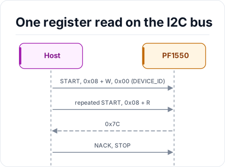
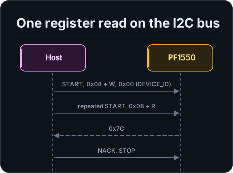
Figure description and sources
Participants, left to right: Host and PF1550. The steps run from top to bottom. Host sends START, 0x08 + W, 0x00 (DEVICE_ID) to PF1550. Host sends repeated START, 0x08 + R to PF1550. PF1550 returns 0x7C to Host. Host sends NACK, STOP to PF1550.
Drawn from: docs/model/i2c-register-read.seq.yml.
An address that nothing acknowledges (no chip, no power, a wrong address) is reported as Error::NoDevice when your
port has the optional GetLastFailure() hook; without it the driver cannot tell it from another bus fault and returns
Bus.
Power
The PF1550 powers itself from VSYS and VBUSIN; the driver has no supply of its own to manage. The limits the driver needs from you describe what the cell and the loads tolerate (Configuration).
| Rail | What the datasheet gives | Driver |
|---|---|---|
| VBUSIN | VUVLO rising 3.8 V to 4.2 V (valid above it) up to OVLO rising 6.0 V to 7.0 V (Table 5; ambiguity C52) | Status only (VbusFlags) |
| VBATT | Single Li-ion cell, charge voltage 3.5 V to 4.44 V | Limits::cell_max_mv |
| VDDIO | 1.7 V to 3.3 V | The port's concern |
| SW1, SW2, SW3 | Programmable bucks | Limits::rail[...] |
| LDO1 to LDO3, VREFDDR | Programmable LDOs, fixed reference | Limits::rail[...] |
| LICELL | Coin cell, charged to 1.8 V to 3.3 V | Limits::coin_cell_max_mv |
Reference application circuit
The datasheet's example schematic (section 13.1, p. 133) shows the power connections: the charger input, the battery, the three bucks with their inductors, the LDOs and their capacitors, the thermistor, the LED and the coin cell. It is not redrawn here. The figure below is only the control connections of a host, as the driver uses them; the resistor values are typical and marked as not confirmed.
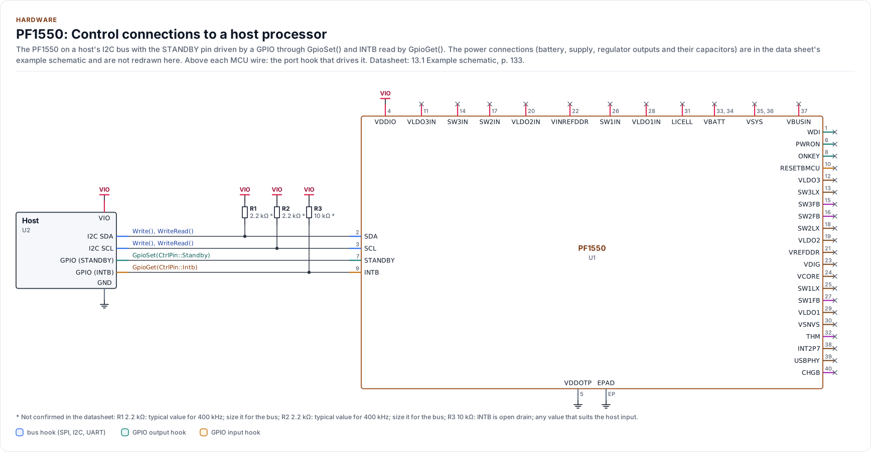
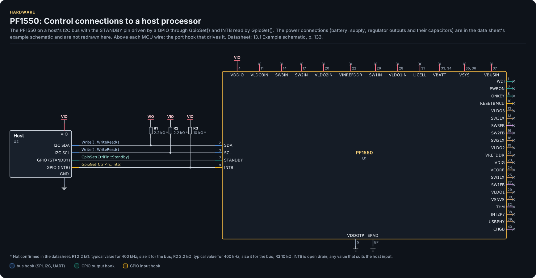
Figure description and sources
A schematic. The MCU is on the left, each of its pins level with the chip pin it connects to; above each wire is the hook of the driver's port that drives or reads it. Supply pins point up to their supply and decoupling, ground pins down. Pins on the right carry the loads and the pins tied to a supply or ground; a cross marks a pin left open. A dot is a junction; wires that cross without a dot are not connected.
Drawn from: docs/hardware.yml; inc/pf1550_i2c_interface.hpp.
| Part | Kind | Value | Connects | Datasheet |
|---|---|---|---|---|
| U2 | Host | - | VIO: VIO, GND: GND, SDA: SDA, SCL: SCL, STBY: STANDBY, IRQ: INTB | 13.1, p. 133 |
| R1 | resistor | 2.2 kΩ (not confirmed: typical value for 400 kHz; size it for the bus) | VIO, SDA | 13.1, p. 133 |
| R2 | resistor | 2.2 kΩ (not confirmed: typical value for 400 kHz; size it for the bus) | VIO, SCL | 13.1, p. 133 |
| R3 | resistor | 10 kΩ (not confirmed: INTB is open drain; any value that suits the host input) | VIO, INTB | 13.1, p. 133 |
Export a circuit for a schematic or PCB tool: kokeb-docs hardware --kicad-netlist OUT.net --circuit typical.
Silicon and options
ReadVariant() returns DEVICE_ID, OTP_FLAVOR, SILICON_REV and the address code. The ten orderable options A0
to A9 differ in their OTP start-up values (Table 85): output voltages, the power-up order, the charger's start-up
mode, the input current limit and whether DVS is enabled. The driver reports the option and the sequencer helpers
model the power-up order of A1 to A9 (API guide).
- A0 parts are "not programmed, internal validation only" (Table 1 footnote). The driver supports reading them and assumes nothing about their start-up values.
SILICON_REVis stored raw and no decision is made on it: the datasheet's text and its register bitmap disagree on the reset value (ambiguity C22).- The OTP image itself is not readable over I2C in the public datasheet, so the driver cannot read the fuses back; it
asks you for the two OTP facts it needs (
BuckConfig::dvs, the declared DVS mode) and reports the rest from the option byte. See Datasheet map.
Reference documents
The datasheet:
PF1550 datasheet. Every pin, setting and timing on this page cites
a section of it; its revision, its SHA-256 and the sections each page relies on are in
docs/datasheets.yml.
| Document | Revision | Get it |
|---|---|---|
| Datasheet: PF1550 Power management integrated circuit (PMIC) for low power application processors (NXP Semiconductors PF1550) | 7, 2021-09-29 | vendor page |
Written against these revisions; the SHA-256 of each file is in docs/datasheets.yml. Where each part
of the driver is in the datasheet: Datasheet map.
| Also useful | Contents |
|---|---|
inc/pf1550_registers.hpp |
The register map as the driver uses it, with datasheet table numbers |
inc/pf1550_sequencer.hpp |
The start-up options and the sequencer timing as constexpr data |