Figures
Every figure on this site is drawn by a Python module from facts extracted from the code, so it is rebuilt,
not redrawn, when the code changes. CI runs kokeb-docs figures --check and fails when a
committed figure no longer matches the code. Each figure below lists the files it is drawn from.
One channel write and its outcomes
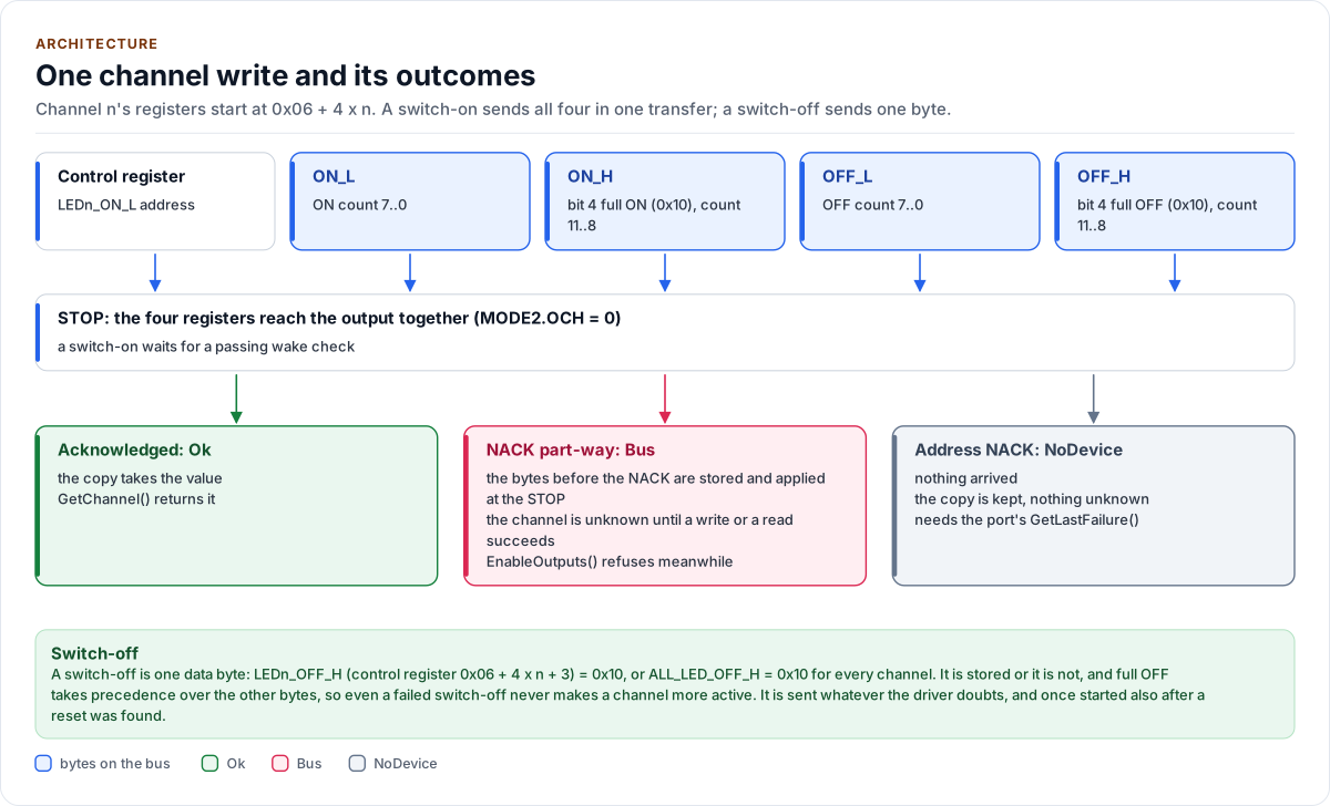
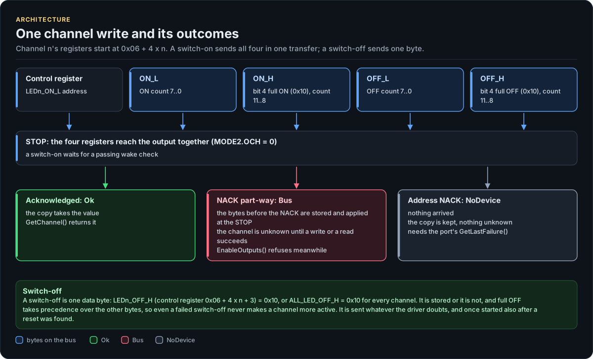
Figure description and sources
Top, the transfer the driver sends for a switch-on (SetDuty(), SetPulseWidthUs(), SetFullOn(), SetPwm()): the control register LEDn_ON_L, then ON_L, ON_H, OFF_L and OFF_H, with auto-increment. With MODE2.OCH = 0, which the driver always keeps, the bytes reach the output together at the STOP. Below, the outcomes: an acknowledged transfer updates the driver's copy; a NACK part-way leaves the bytes before it stored and applied at the STOP, so the channel may hold old, new or mixed values and becomes unknown; an address NACK proves nothing arrived. The band at the bottom is the switch-off: one data byte, LEDn_OFF_H = 0x10, stored or not, and full OFF takes precedence, so a switch-off never makes a channel more active, even when it fails; it is sent whatever the driver doubts.
Drawn from: src/pca9685.ipp applyOne, switchOn, switchOff, afterSwitchOff, writeChannels; inc/pca9685_registers.hpp kLed0OnL, kBytesPerChannel, kLedFull; figure module docs/diagrams/figures/channel-write.py.
Figure module: docs/diagrams/figures/channel-write.py
Drawn from:
applyOne, switchOn, switchOff, afterSwitchOff, writeChannelsinsrc/pca9685.ippkLed0OnL, kBytesPerChannel, kLedFullininc/pca9685_registers.hpp
Inside the PCA9685
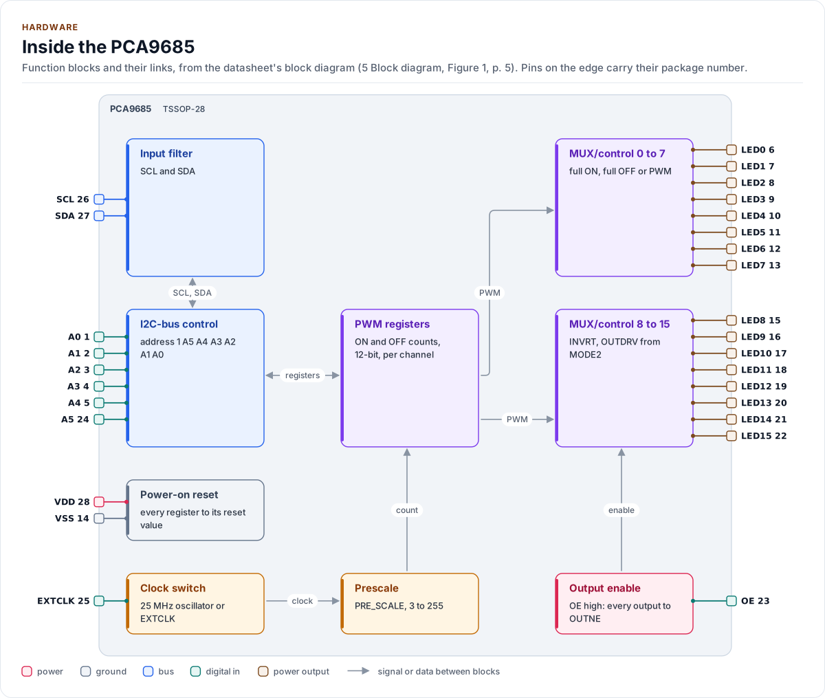
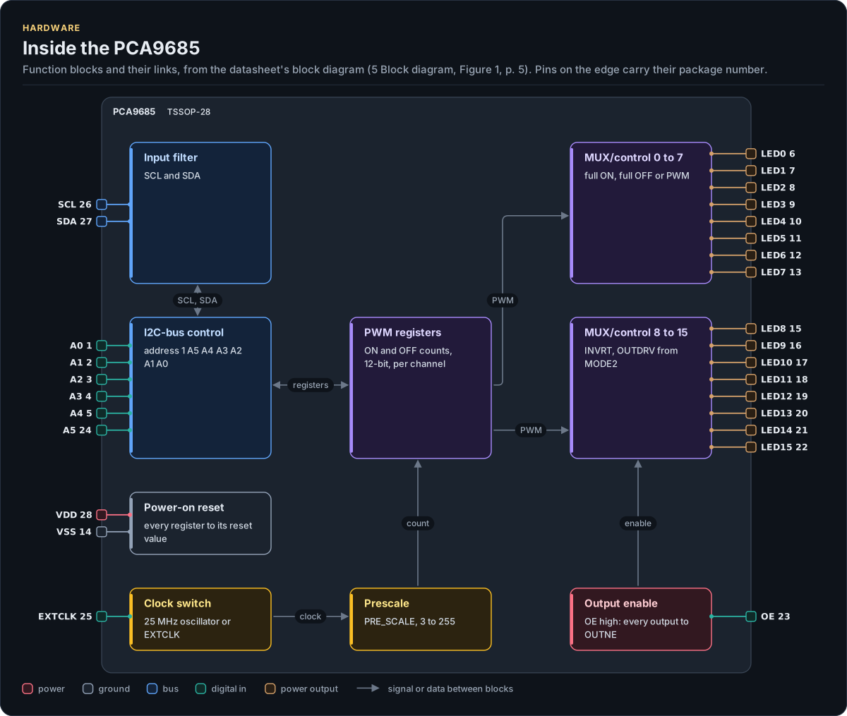
Figure description and sources
The PCA9685's function blocks inside its outline. Arrows between blocks carry signals or data in the direction they point (both ways where they have two heads). The package pins stand on the left and right edges with their numbers, each wired to the block it reaches.
Drawn from: docs/hardware.yml; inc/pca9685_i2c_interface.hpp.
Hardware description: docs/hardware.yml
Drawn from:
PCA9685: Typical application
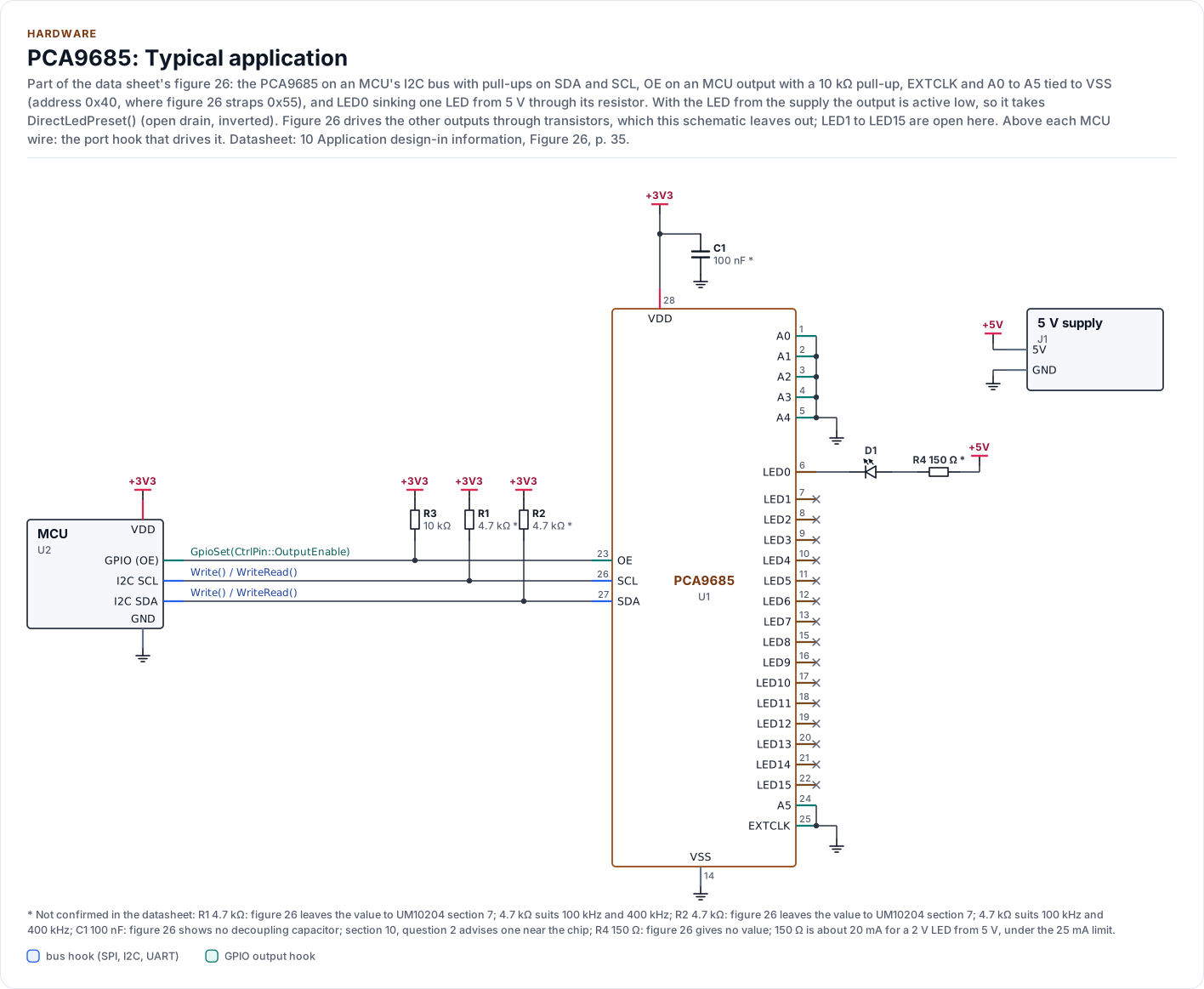
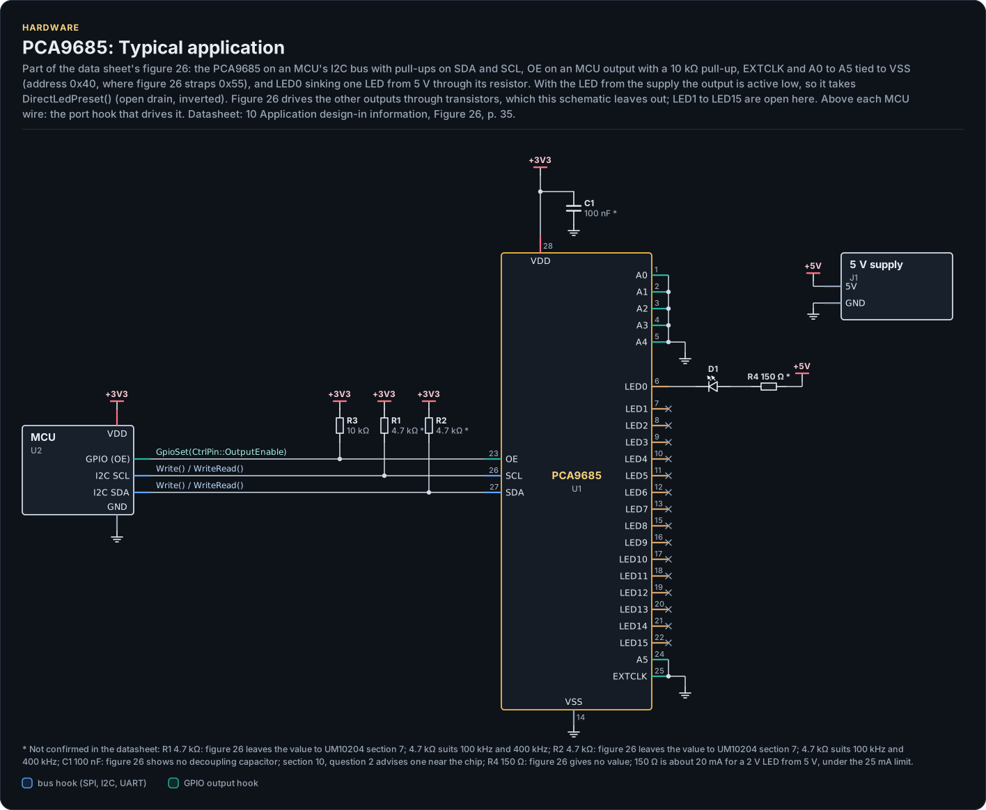
Figure description and sources
A schematic. The MCU is on the left, each of its pins level with the chip pin it connects to; above each wire is the hook of the driver's port that drives or reads it. Supply pins point up to their supply and decoupling, ground pins down. Pins on the right carry the loads and the pins tied to a supply or ground; a cross marks a pin left open. A dot is a junction; wires that cross without a dot are not connected.
Drawn from: docs/hardware.yml; inc/pca9685_i2c_interface.hpp.
Hardware description: docs/hardware.yml
Drawn from:
PCA9685 pinout, TSSOP-28
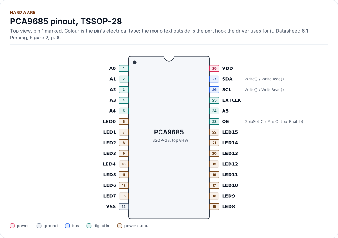
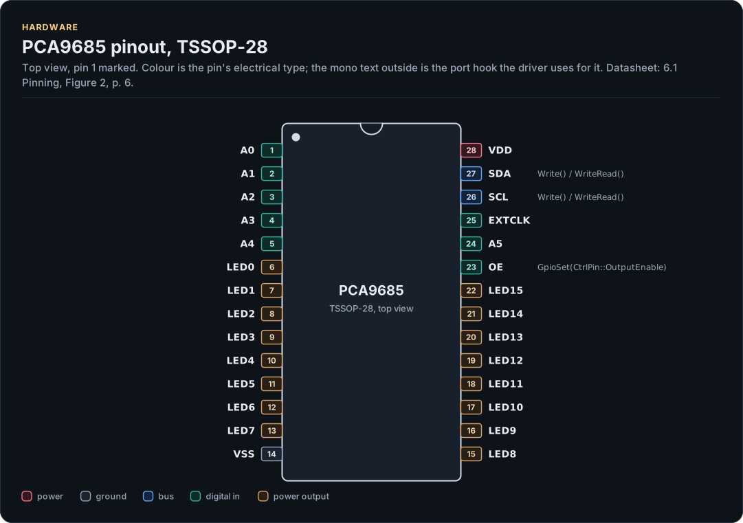
Figure description and sources
The PCA9685 seen from the top, in its TSSOP-28 package. Pin 1 is marked by the dot; the numbers run counter-clockwise from it. Each pad is coloured by the pin's electrical type (legend below). Next to it is the pin's name and, in mono, the hook of the driver's port that drives or reads it; a pin without a hook is not used by the driver.
Drawn from: docs/hardware.yml; inc/pca9685_i2c_interface.hpp.
Hardware description: docs/hardware.yml
Drawn from:
The layers, one of them yours
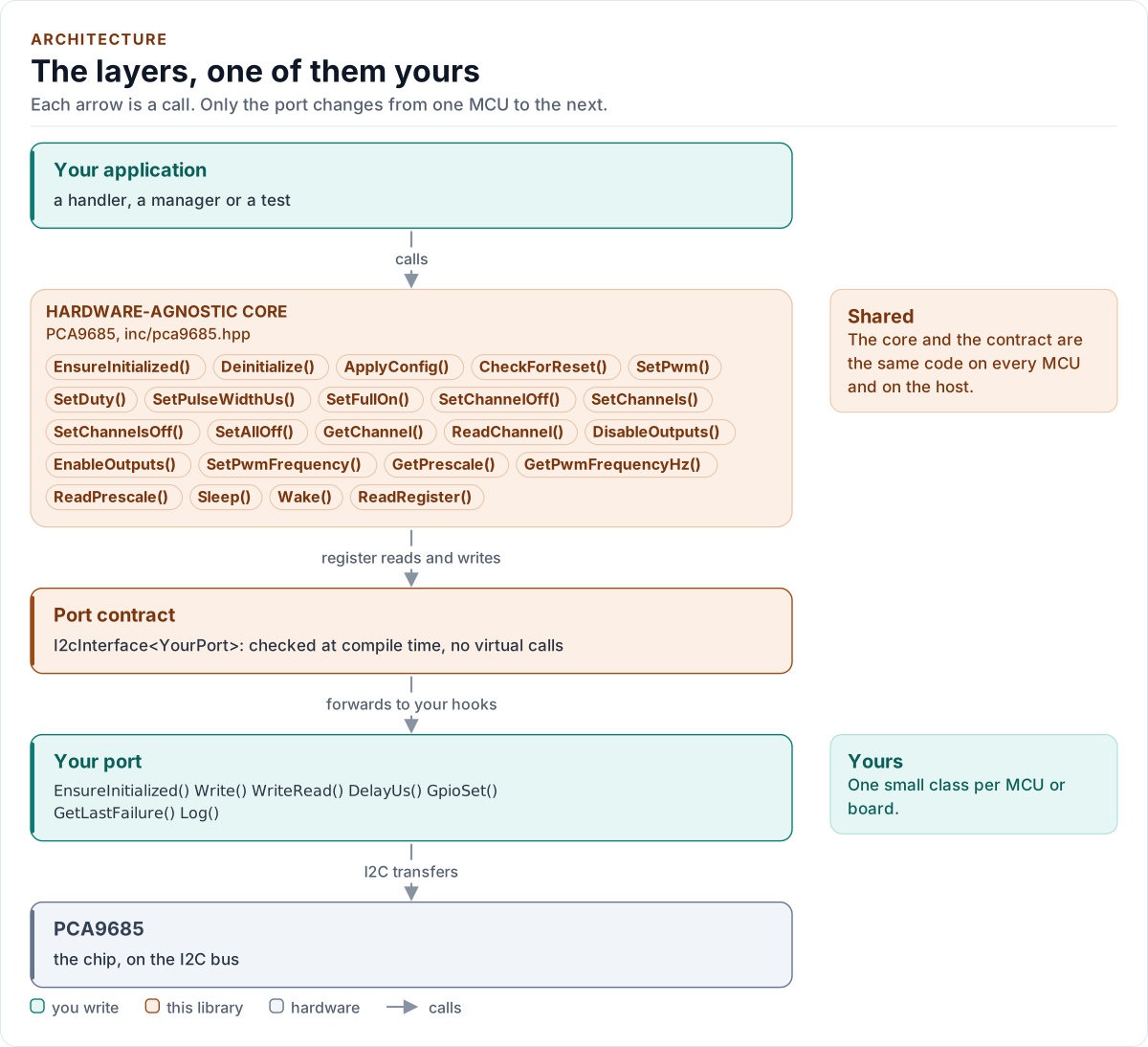
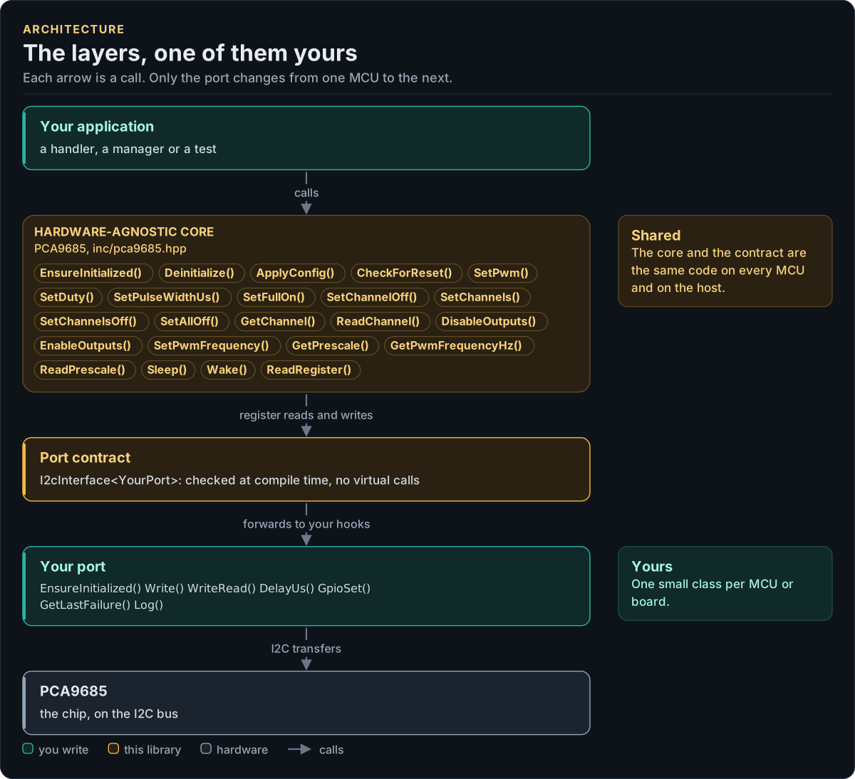
Figure description and sources
Top to bottom, each arrow is a call. Your application calls one object, whose public calls are listed from the umbrella header in inc/. The core turns each call into register reads and writes and hands them to the port contract (the CRTP base in inc/*_interface.hpp), which forwards them, at compile time, to the hooks of the port class you write; your port moves the bytes on the bus. The notes on the right say which layers stay the same on every MCU and which one you write. A library without a port contract has only the first two layers.
Drawn from: inc/pca9685.hpp public calls; inc/pca9685_i2c_interface.hpp I2cInterface; figure module docs/diagrams/figures/driver-layers.py.
Figure module: docs/diagrams/figures/driver-layers.py
Drawn from:
public callsininc/pca9685.hppI2cInterfaceininc/pca9685_i2c_interface.hpp
From the registers to the pin
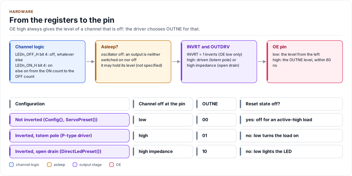
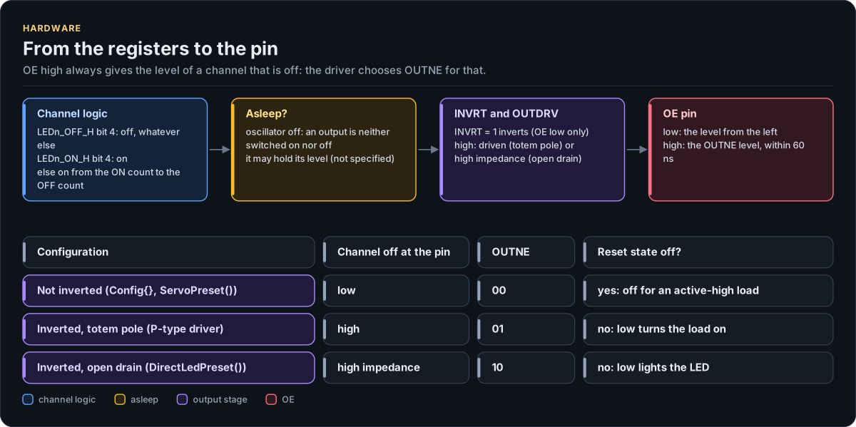
Figure description and sources
Left to right, what decides the level of output LEDn (tables 6, 7 and 11). The channel logic is off when LEDn_OFF_H bit 4 is set, whatever else the registers hold; otherwise on when LEDn_ON_H bit 4 is set; otherwise asserted from the ON count to the OFF count of the 12-bit counter. Asleep, the oscillator is off and an output can be neither switched on nor off. INVRT inverts the logic while OE is low; OUTDRV makes a high level a driven high (totem pole) or high impedance (open drain). OE high replaces everything with the OUTNE level, which the driver sets to the level of a channel that is off. The table at the bottom gives that level for each configuration, and whether the reset state (not inverted, OUTNE = 00) is off for the load.
Drawn from: inc/pca9685.hpp OffLevelOutne, Mode2Value; inc/pca9685_registers.hpp kOutneLow, kOutneHigh, kOutneHiZ, kLedFull; src/pca9685.ipp applyOne; figure module docs/diagrams/figures/output-path.py.
Figure module: docs/diagrams/figures/output-path.py
Drawn from:
OffLevelOutne, Mode2Valueininc/pca9685.hppkOutneLow, kOutneHigh, kOutneHiZ, kLedFullininc/pca9685_registers.hppapplyOneinsrc/pca9685.ipp
Sleep, wake and restart
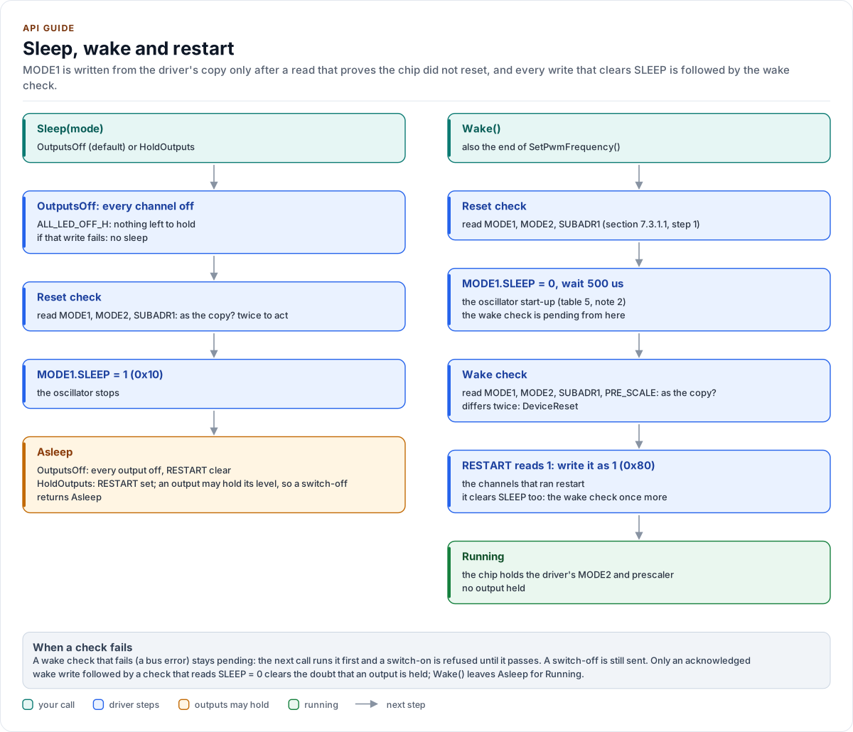
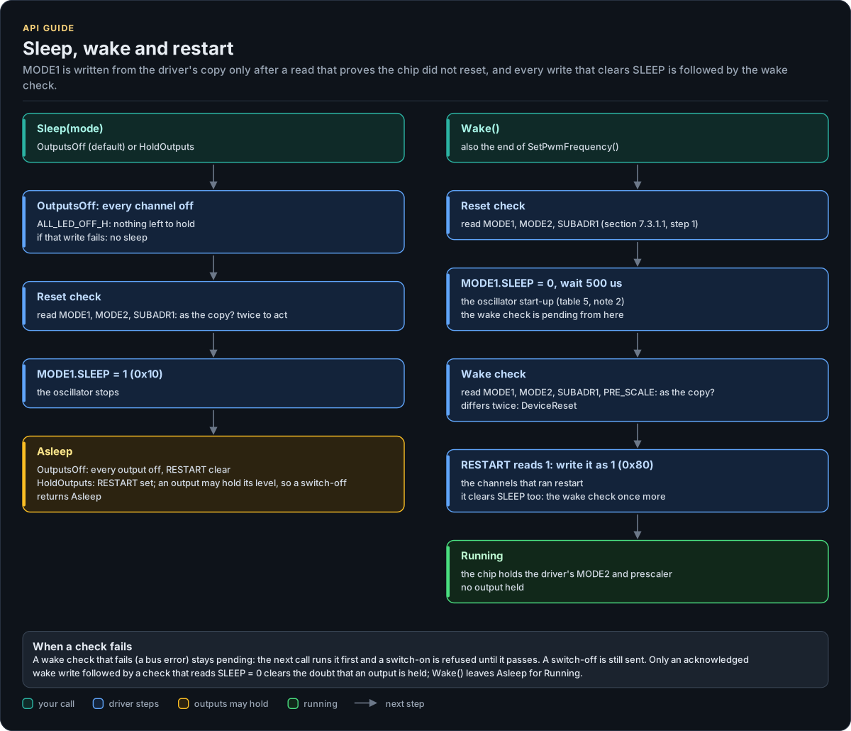
Figure description and sources
Left, the two ways to sleep. SleepMode::OutputsOff writes ALL_LED_OFF first (the orderly shutdown of section 7.3.1.1), so nothing is held and RESTART stays clear; SleepMode::HoldOutputs sleeps with the channels running, so RESTART sets and an output may hold its level while the oscillator is off. Both read MODE1 and MODE2 first, the reset check, before MODE1 is written from the driver's copy. Right, the wake: the reset check, MODE1 with SLEEP = 0, the oscillator start-up wait, then the wake check (MODE1, MODE2 and PRE_SCALE compared with the copy); when RESTART reads 1 it is written back as 1, which restarts the channels, and because that write clears SLEEP too the wake check runs once more. SetPwmFrequency() is a sleep, a PRE_SCALE write and read-back, and this wake. The band at the bottom says what a failed check leaves.
Drawn from: src/pca9685.ipp Sleep, Wake, wakeSequence, completeWakeCheck, verifyRunning, SetPwmFrequency, changePrescale; inc/pca9685_registers.hpp kMode1Sleep, kMode1Restart; inc/pca9685_types.hpp kOscillatorStartUs; figure module docs/diagrams/figures/sleep-restart.py.
Figure module: docs/diagrams/figures/sleep-restart.py
Drawn from:
Sleep, Wake, wakeSequence, completeWakeCheck, verifyRunning, SetPwmFrequency, changePrescaleinsrc/pca9685.ippkMode1Sleep, kMode1Restartininc/pca9685_registers.hppkOscillatorStartUsininc/pca9685_types.hpp
What EnsureInitialized() does
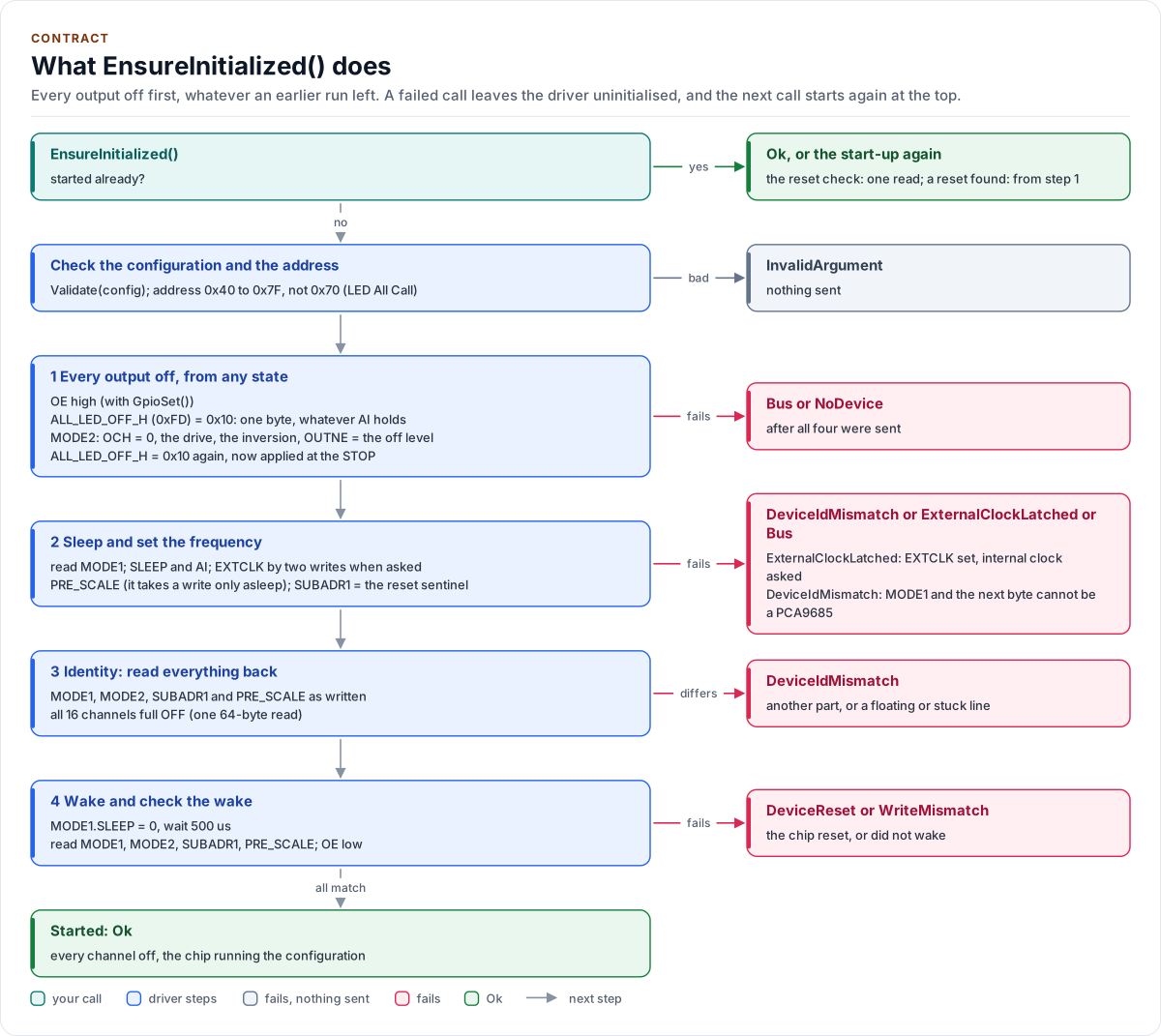
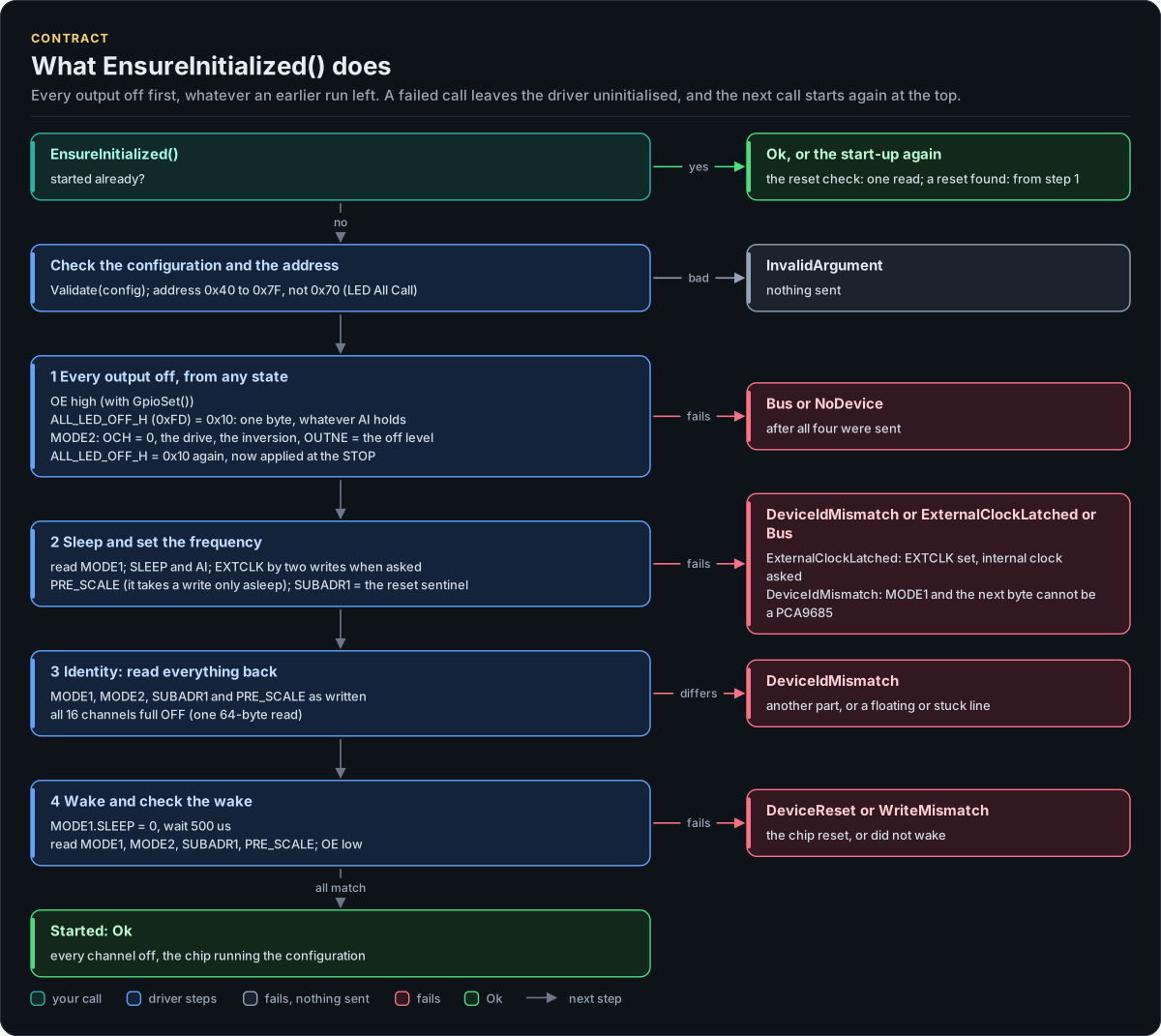
Figure description and sources
Top to bottom on the left, the steps of the first EnsureInitialized() call; once it has succeeded a later call runs the reset check (one read) and returns Ok, or starts again at the top when the chip reset. The configuration and the address are checked before any I/O. Step 1 switches everything off whatever an earlier run left: OE high, then one-byte ALL_LED_OFF_H writes before and after MODE2, which sets OCH = 0 so the second one reaches the outputs at its STOP; all four are sent even when one fails. Step 2 reads MODE1, puts the chip to sleep with auto-increment on (EXTCLK by the two-write sequence when asked), writes PRE_SCALE, which only takes a write asleep, and the SUBADR1 reset sentinel. Step 3 is the identity check: the chip has no ID register, so MODE1, MODE2, SUBADR1 and PRE_SCALE must read back what was written and every channel full OFF. Step 4 wakes the oscillator, waits its start-up, runs the wake check (MODE1, MODE2, SUBADR1 and PRE_SCALE once more) and enables OE. Each card on the right is the error a step returns; after any failure the driver stays uninitialised and the next call starts at the top.
Drawn from: src/pca9685.ipp EnsureInitialized, initialize, enterSafeState, configureClock, checkIdentity, wakeSequence, addressValid; inc/pca9685_types.hpp kMinI2cAddress, kMaxI2cAddress, kAllCallAddress, kOscillatorStartUs; inc/pca9685_registers.hpp kAllLedOffH, kLedFull; figure module docs/diagrams/figures/start-up.py.
Figure module: docs/diagrams/figures/start-up.py
Drawn from:
EnsureInitialized, initialize, enterSafeState, configureClock, checkIdentity, wakeSequence, addressValidinsrc/pca9685.ippkMinI2cAddress, kMaxI2cAddress, kAllCallAddress, kOscillatorStartUsininc/pca9685_types.hppkAllLedOffH, kLedFullininc/pca9685_registers.hpp