Hardware
The FDO2 module's connector, signal levels, supply and timing, as the driver uses them.
Datasheet sections this page relies on
- Measuring range, accuracy and warm-up: PyroScience Datasheet_FDO2-G2 v5, 2 Specifications, Analytical Performance, p. 5
- Supply voltage and current: PyroScience Datasheet_FDO2-G2 v5, 2 Specifications, Interface, p. 6
- Temperature and pressure limits, humidity: PyroScience Datasheet_FDO2-G2 v5, 2 Specifications, Environment, p. 6
- Mechanics, connector part and weight: PyroScience Datasheet_FDO2-G2 v5, 2 Specifications, Mechanical, p. 7
- Cross-sensitivity and chemical compatibility: PyroScience Datasheet_FDO2-G2 v5, 3 Cross-Sensitivity and Chemical Compatibility, p. 8
- Power-up time: PyroScience Datasheet_FDO2-G2 v5, 4 Communication Interface, p. 10
- Connector, pins and signal levels: PyroScience Datasheet_FDO2-G2 v5, 7 Mechanical Dimensions and Electrical Interface, drawing and pin table, p. 20
- Mechanical drawing: PyroScience Datasheet_FDO2-G2 v5, 7 Mechanical Dimensions and Electrical Interface, drawings, p. 20
- Supply below 3.3 V and readings: PyroScience Datasheet_FDO2 v21, 2 Specifications, Interface, WARNING, p. 6
- UART levels: 3.0 V, 3.3 V maximum on RXD: PyroScience Datasheet_FDO2 v21, 6.2 Voltage Tolerance of UART RX Pin (ERRATA), p. 19
- Replacement of the FDO2 by the FDO2-G2: PyroScience PCN-FDO2-002 n/a, Product change notification, text, p. 1
- Flow-through cell accessory: PyroScience Data Sheet_FDO2_FTC n/a, Flow-through cell data sheet, whole document, p. 1
All of them, with the driver API for each: Datasheet map.
RXD tolerates 3.3 V at most
The module's UART runs at 3.0 V. The RXD pin (pin 3) must not see more than 3.3 V. A controller with 5 V
outputs needs a divider or a level shifter in front of RXD (the 5 V circuit). The legacy
FDO2's datasheet (section 6.2, all modules) corrects an earlier "5 V tolerant" statement, found in versions up to
17 (April 2023), to "max. 3.3 V".
The driver cannot check the wiring; the port examples assert kMaxLogicLevelMv so the number is in your code.
Pins
The module has a four-pin connector. The mating plug is the vendor's to name (see section 7 of the datasheet); this page does not give a part number. Not verified on hardware: the wiring below follows the datasheet.
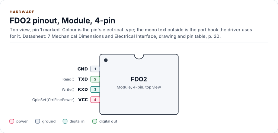
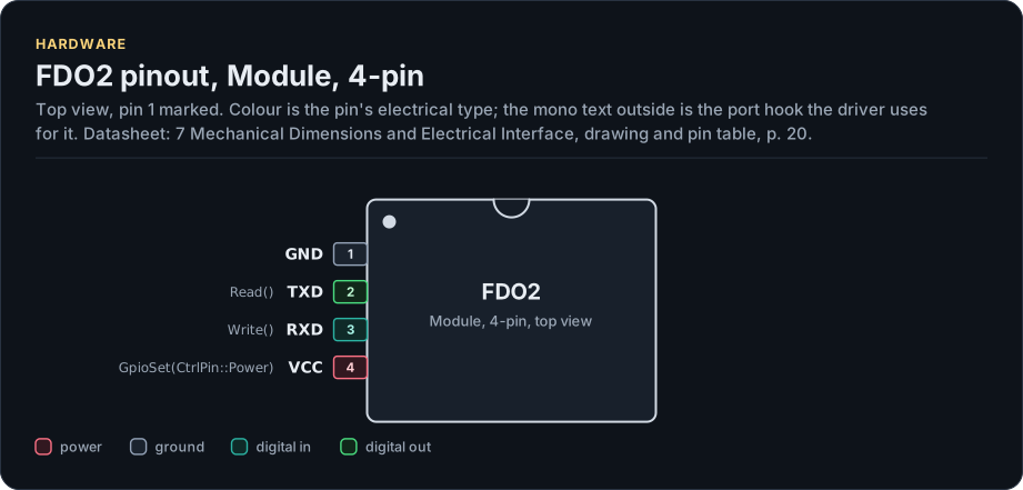
Figure description and sources
The FDO2 seen from the top, in its Module, 4-pin package. Pin 1 is marked by the dot; the numbers run counter-clockwise from it. Each pad is coloured by the pin's electrical type (legend below). Next to it is the pin's name and, in mono, the hook of the driver's port that drives or reads it; a pin without a hook is not used by the driver.
Drawn from: docs/hardware.yml; inc/fdo2_uart_interface.hpp.
Module, 4-pin, 4 pins (7 Mechanical Dimensions and Electrical Interface, drawing and pin table, p. 20).
| Pin | Name | Type (domain) | Function | Driver hook | If unused | Datasheet |
|---|---|---|---|---|---|---|
| 1 | GND |
ground | Ground | - | - | 7, p. 20 |
| 2 | TXD |
digital out (UART 3.0 V) | Module transmit: 3.0 V UART data to the host (host RX) | Read() |
Leave open | 7, p. 20 |
| 3 | RXD |
digital in (UART 3.0 V) | Module receive: UART data from the host, 3.0 V levels, absolute maximum 3.3 V (host TX) | Write() |
- | 7, p. 20 |
| 4 | VCC |
power (VCC) | Supply 3.3 V to 5.0 V; below 3.3 V the oxygen readings can be wrong. Optionally switched by the port's power hook | GpioSet(CtrlPin::Power) |
- | 7, p. 20 |
Source of this table and of the chip figures: docs/hardware.yml.
Supply
VCC takes 3.3 V to 5.0 V. Below 3.3 V the oxygen readings can be wrong, and the module has no supply reading, so
the driver cannot detect it. After power-up the module needs about one second before it answers; the driver waits
Config::power_up_ms (1500 ms by default). Readings in the first three minutes have reduced accuracy:
Oxygen::warming_up is true for that time.
A load switch on the supply is optional. If your port has GpioSet(CtrlPin::Power, ...), PowerCycle() switches
the supply off for Config::power_off_ms and on again, and EnsureInitialized() waits the power-up time.
Bus settings
| Setting | Value |
|---|---|
| Baud rate | 19200 after every power-up; SetBaudRate() can raise it until the next power-up |
| Frame | 8 data bits, no parity, 1 stop bit, no handshake |
| Levels | 3.0 V; 3.3 V absolute maximum on RXD |
| Messages | ASCII, ended by one carriage return |
| Receive buffer | At least 800 bytes (kRxBufferBytes): the longest reply |
The commands are on the Protocol page.
Mechanical
The module is cylindrical, 28.5 mm in diameter and 27.5 mm with the connector (datasheet section 2 and 7). Its body is drawn in the outline figure as a square of that size, because the figure system has no round bodies yet; see Limitations.
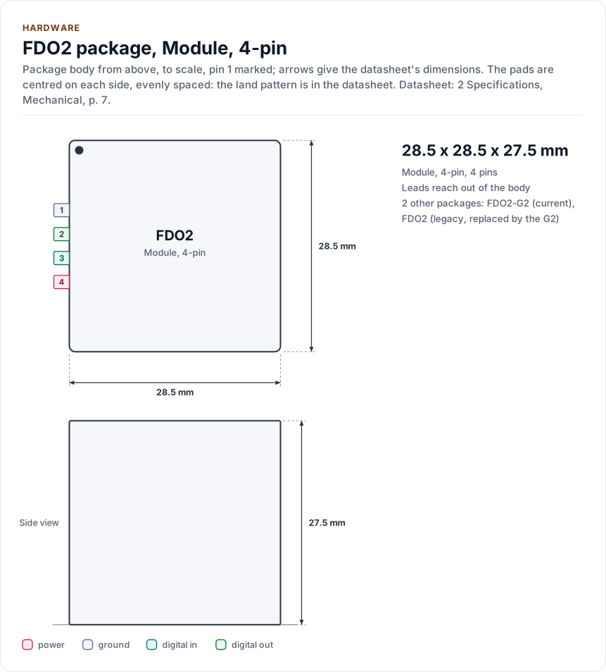
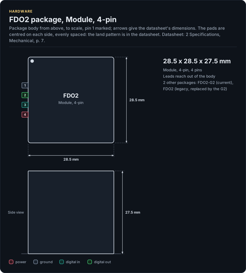
Figure description and sources
The FDO2 package seen from the top and, when the height is known, from the side, drawn to scale: 28.5 x 28.5 x 27.5 mm. The arrows carry the datasheet's dimensions, the dot marks pin 1 and the pads are numbered counter-clockwise from it, coloured by the pin's electrical type (legend below). Pads sit centred on each side, evenly spaced; the datasheet's land pattern is the reference for a board.
Drawn from: docs/hardware.yml; inc/fdo2_uart_interface.hpp.
Inside the module
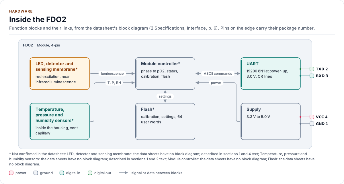
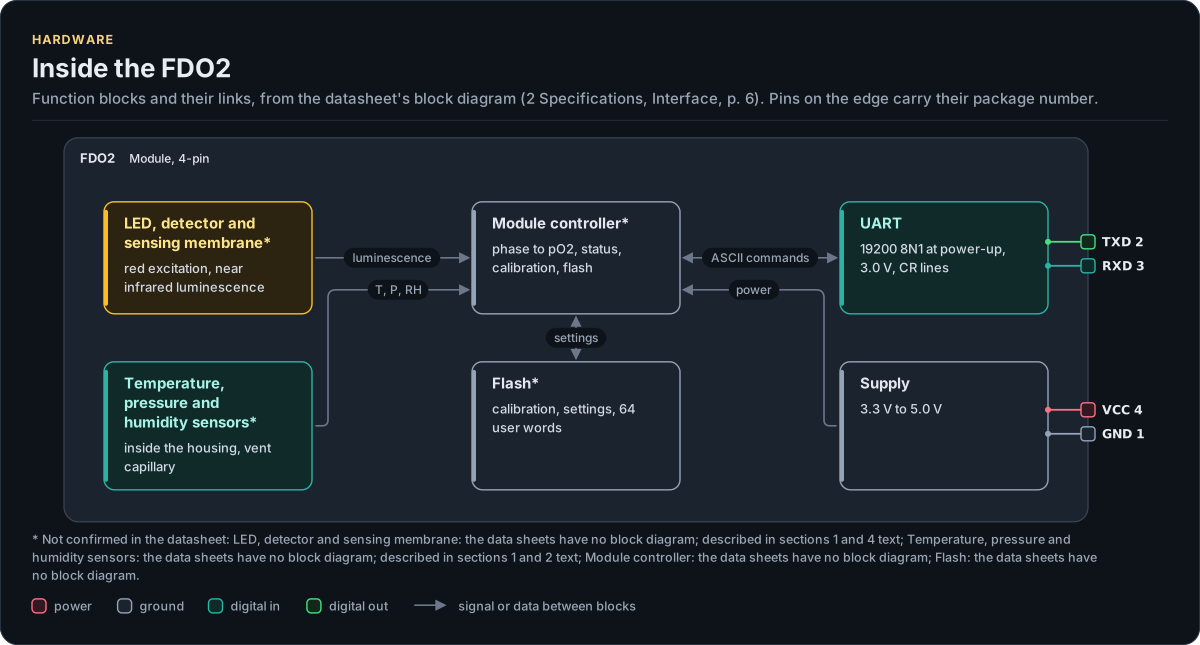
Figure description and sources
The FDO2's function blocks inside its outline. Arrows between blocks carry signals or data in the direction they point (both ways where they have two heads). The package pins stand on the left and right edges with their numbers, each wired to the block it reaches.
Drawn from: docs/hardware.yml; inc/fdo2_uart_interface.hpp.
The datasheets have no block diagram; this one is drawn from their text, and its blocks are marked as unverified in
hardware.yml.
Circuits
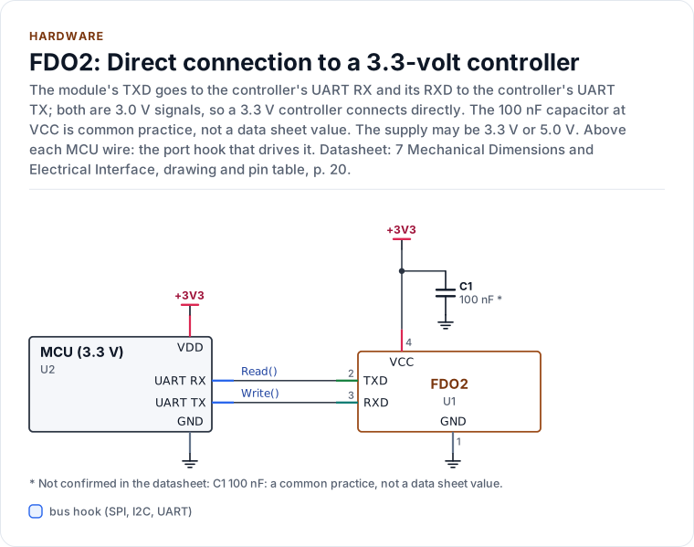
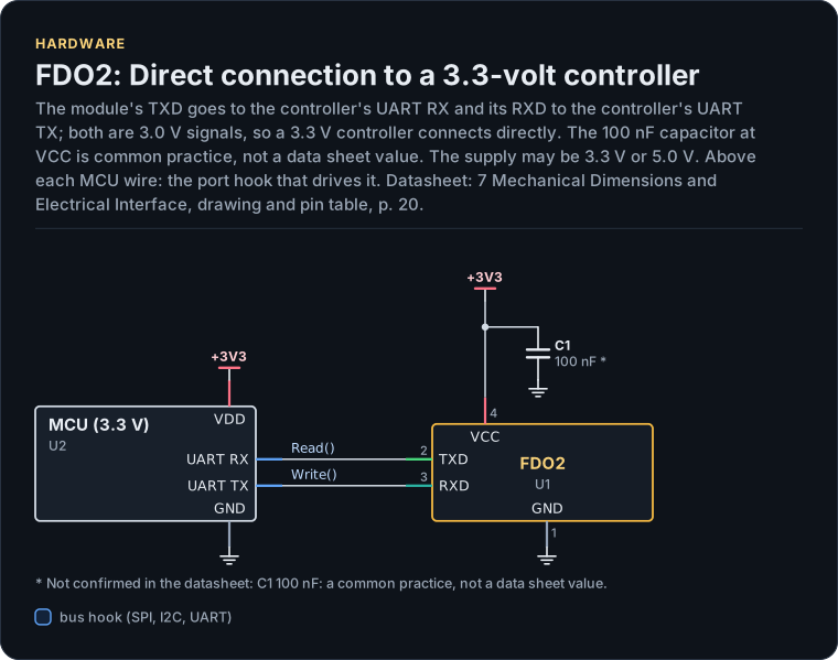
Figure description and sources
A schematic. The MCU is on the left, each of its pins level with the chip pin it connects to; above each wire is the hook of the driver's port that drives or reads it. Supply pins point up to their supply and decoupling, ground pins down. Pins on the right carry the loads and the pins tied to a supply or ground; a cross marks a pin left open. A dot is a junction; wires that cross without a dot are not connected.
Drawn from: docs/hardware.yml; inc/fdo2_uart_interface.hpp.
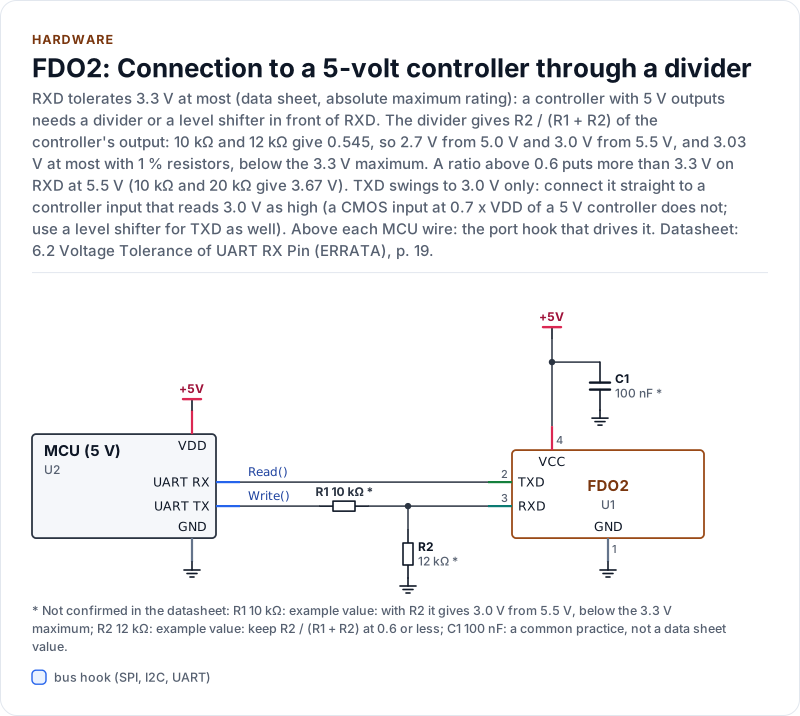
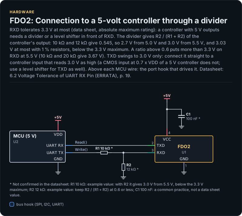
Figure description and sources
A schematic. The MCU is on the left, each of its pins level with the chip pin it connects to; above each wire is the hook of the driver's port that drives or reads it. Supply pins point up to their supply and decoupling, ground pins down. Pins on the right carry the loads and the pins tied to a supply or ground; a cross marks a pin left open. A dot is a junction; wires that cross without a dot are not connected.
Drawn from: docs/hardware.yml; inc/fdo2_uart_interface.hpp.
Direct connection to a 3.3-volt controller (figure chip-circuit-direct)
| Part | Kind | Value | Connects | Datasheet |
|---|---|---|---|---|
| U2 | MCU (3.3 V) | - | VDD: +3V3, GND: GND, TX: MCU TX to RXD, RX: TXD to MCU RX | 7, p. 20 |
| C1 | capacitor | 100 nF (not confirmed: a common practice, not a data sheet value) | +3V3, GND | 7, p. 20 |
Connection to a 5-volt controller through a divider (figure chip-circuit-shifted)
| Part | Kind | Value | Connects | Datasheet |
|---|---|---|---|---|
| U2 | MCU (5 V) | - | VDD: +5V, GND: GND, TX: MCU TX, RX: TXD to MCU RX | 6.2, p. 19 |
| R1 | resistor | 10 kΩ (not confirmed: example value: with R2 it gives 3.0 V from 5.5 V, below the 3.3 V maximum) | MCU TX, RXD | 6.2, p. 19 |
| R2 | resistor | 12 kΩ (not confirmed: example value: keep R2 / (R1 + R2) at 0.6 or less) | GND, RXD | 6.2, p. 19 |
| C1 | capacitor | 100 nF (not confirmed: a common practice, not a data sheet value) | +5V, GND | 6.2, p. 19 |
Export a circuit for a schematic or PCB tool: kokeb-docs hardware --kicad-netlist OUT.net --circuit direct.
The 100 nF capacitor is common practice, not a datasheet value. The divider values are an example.
Datasheet
| Document | Revision | Get it |
|---|---|---|
| Datasheet: FDO2-G2 Optical Oxygen Sensor Data Sheet (PyroScience Datasheet_FDO2-G2) | v5, 2026-03 | PDF · vendor page |
| Datasheet: FDO2 Optical Oxygen Sensor Data Sheet (legacy part) (PyroScience Datasheet_FDO2) | v21, 2025-06 | PDF · vendor page |
| Product change notification: Low-pass filter and noise erratum (PyroScience PCN-FDO2-G2-001) | n/a, 2026-03 | PDF · vendor page |
| Product change notification: FDO2 replaced by FDO2-G2 (PyroScience PCN-FDO2-002) | n/a, 2025-05 | PDF · vendor page |
| Quick start guide: Quick Start FDO2-G2 evaluation kit (PyroScience Quick_Start_FDO2-G2) | v1.00, n/a | PDF · vendor page |
| Datasheet: FDO2-FTC flow-through cell data sheet (accessory) (PyroScience Data Sheet_FDO2_FTC) | n/a, n/a | PDF · vendor page |
| Datasheet: FDO2-EXT Modbus and analog extension module data sheet (PyroScience Datasheet_FDO2-EXT) | v5, 2025-07 | PDF · vendor page |
Written against these revisions; the SHA-256 of each file is in docs/datasheets.yml. Where each part
of the driver is in the datasheet: Datasheet map.
Next: Protocol.