Hardware
The BMP581's package, pins, connections, bus settings, timing and power, as the driver relies on them.
Datasheet sections this page relies on
From Bosch Sensortec BST-BMP581-DS004-13 1.13:
- Measurement range, resolution and accuracy: 2 Specification; Table 1 Pressure Performance; Table 2 Temperature Performance, p. 8
- Supplies, timing and conversion times: 2 Specification; Table 4 Electrical characteristics, p. 10
- Block diagram and power management: 4.1 Block diagram; 4.2 Power management, p. 14
- INT pin: 4.7.3 Interrupt pin, p. 27
- Interface selection (I2C, SPI): 5.1 Protocol Selection; Table 16, p. 31
- I2C protocol and addresses: 5.6 I2C protocol; 5.6.1 I2C write operation; 5.6.2 I2C read operation, p. 38
- Pins and connection diagrams: 6.1 Pin Out; 6.2 Connection Diagrams; Table 28, p. 46
All of them, with the driver API for each: Datasheet map.
Package
A 10-pin metal-lid LGA, 2.0 mm x 2.0 mm, at most 0.8 mm high (table 3). The vent hole is on the lid; keep it open, and keep vias, traces and solder mask out from under the part (section 8.2).
Pins
Top view of figure 23. There is no reset or enable pin: CSB at power-up selects the interface, and the driver resets the chip with a command.
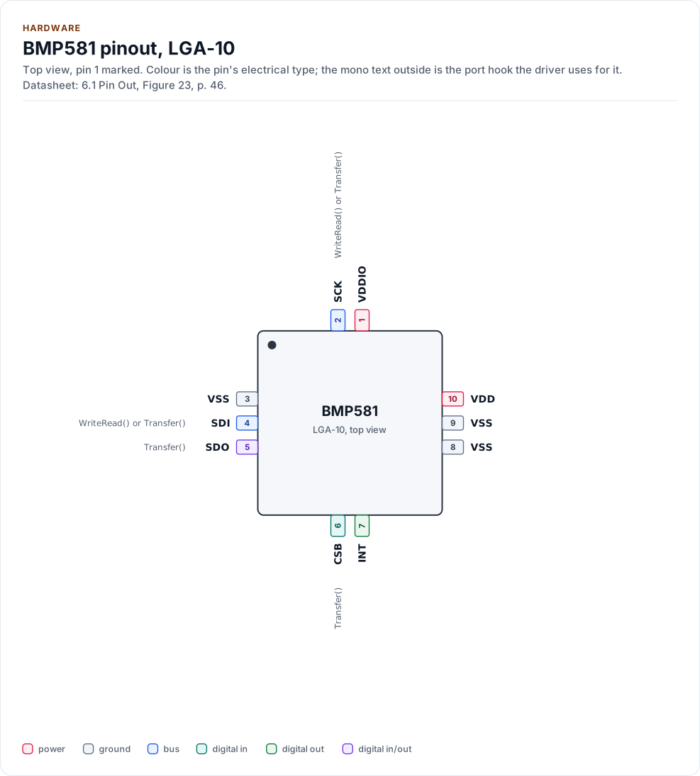
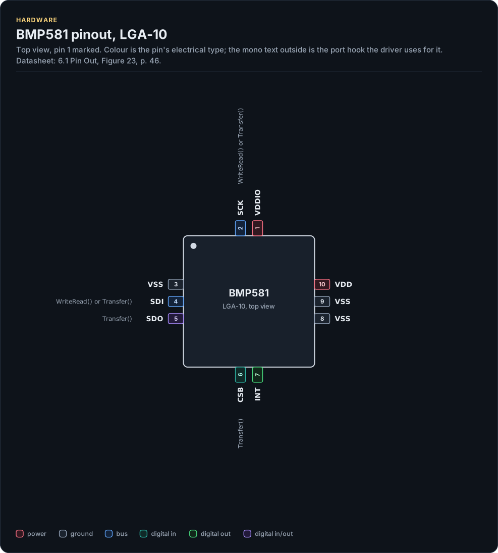
Figure description and sources
The BMP581 seen from the top, in its LGA-10 package. Pin 1 is marked by the dot; the numbers run counter-clockwise from it. Each pad is coloured by the pin's electrical type (legend below). Next to it is the pin's name and, in mono, the hook of the driver's port that drives or reads it; a pin without a hook is not used by the driver.
Drawn from: docs/hardware.yml; inc/bmp581_i2c_interface.hpp; inc/bmp581_spi_interface.hpp.
LGA-10, 10 pins (6.1 Pin Out, Figure 23, p. 46).
| Pin | Name | Type (domain) | Function | Driver hook | If unused | Datasheet |
|---|---|---|---|---|---|---|
| 1 | VDDIO |
power (VDDIO) | Digital interface supply, 1.08 V to 3.6 V; any order with VDD | - | - | 2, p. 10 |
| 2 | SCK |
bus (VDDIO) | Serial clock: I2C SCL, or SPI SCK | WriteRead() or Transfer() |
- | 6.1, p. 46 |
| 3 | VSS |
ground | Ground | - | - | 6.1, p. 46 |
| 4 | SDI |
bus (VDDIO) | Serial data: I2C SDA, or SPI MOSI (SDX); data in and out in 3-wire SPI | WriteRead() or Transfer() |
- | 6.1, p. 46 |
| 5 | SDO |
digital in/out (VDDIO) | SPI MISO; on I2C the address LSB: VSS 0x46, VDDIO 0x47 | Transfer() |
I2C: tie to VSS or VDDIO, never open | 5.6, p. 38 |
| 6 | CSB |
digital in (VDDIO) | SPI chip select, active low; held at VDDIO from power-up selects I2C | Transfer() |
I2C: tie to VDDIO | 5.1, p. 31 |
| 7 | INT |
digital out (VDDIO) | Interrupt output, push-pull or open drain, polarity set by INT_CONFIG | - | Tie to GND with INT_CONFIG.int_en = 0, the reset value | 4.7.3, p. 27 |
| 8 | VSS |
ground | Ground | - | - | 6.1, p. 46 |
| 9 | VSS |
ground | Ground | - | - | 6.1, p. 46 |
| 10 | VDD |
power (VDD) | Analog supply, 1.71 V to 3.6 V; any order with VDDIO | - | - | 2, p. 10 |
Source of this table and of the chip figures: docs/hardware.yml.
Never hold SDI, SDO, SCK or CSB high while VDDIO is off: the current through the protection diodes can damage the part (section 4.2).
Blocks
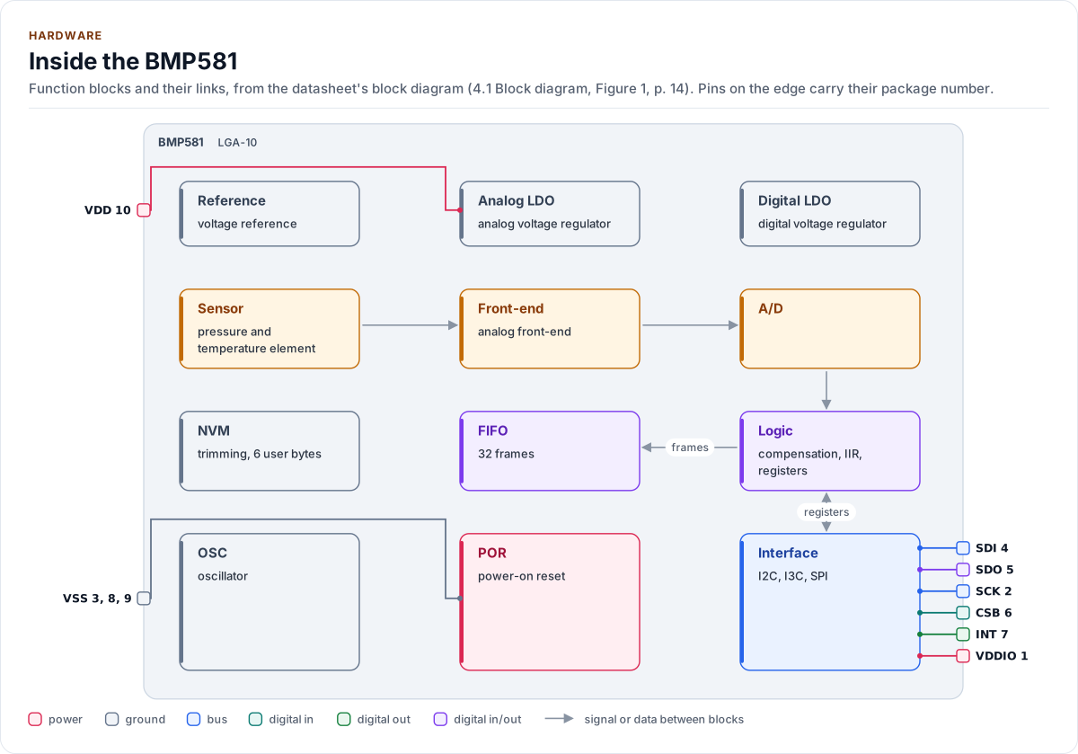
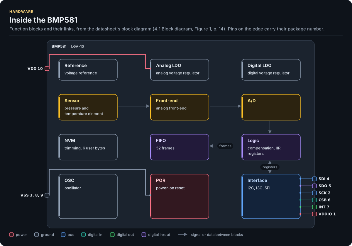
Figure description and sources
The BMP581's function blocks inside its outline. Arrows between blocks carry signals or data in the direction they point (both ways where they have two heads). The package pins stand on the left and right edges with their numbers, each wired to the block it reaches.
Drawn from: docs/hardware.yml; inc/bmp581_i2c_interface.hpp; inc/bmp581_spi_interface.hpp.
The chip compensates both values itself (section 4.1): the data registers and the FIFO hold pressure in pascals and temperature in degrees Celsius as fixed-point numbers, and the driver only converts their scale.
Interface selection
After a power-on or soft reset the interface is in I2C mode (section 5.1). With CSB tied to VDDIO it stays there.
The first CSB low phase with at least 16 SCK edges changes it to SPI until the next reset; that first frame
carries no valid data. The SPI port of the driver sends this dummy read itself, in EnsureInitialized() and again
after its soft reset, because a soft reset returns the interface to I2C (table 16). An I2C board must never pull
CSB low: the chip would leave I2C mode until the next power cycle.
I2C
- Address
0x46with SDO at VSS,0x47with SDO at VDDIO (section 5.6); SDO must not float. - 100 kHz to 1 MHz (table 4): fast mode plus needs a bus capacitance under 100 pF.
- A register read is a write of the address, then a read; the chip keeps the address across a STOP, so a
repeated START or a STOP and START both work (figures 15, 16). The driver calls
WriteRead(). - The soft reset (CMD = 0xB6) is not acknowledged (section 7.36); the driver expects the NACK and proves the reset by the reads that follow.
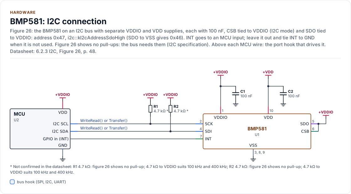
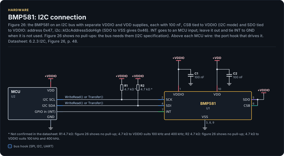
Figure description and sources
A schematic. The MCU is on the left, each of its pins level with the chip pin it connects to; above each wire is the hook of the driver's port that drives or reads it. Supply pins point up to their supply and decoupling, ground pins down. Pins on the right carry the loads and the pins tied to a supply or ground; a cross marks a pin left open. A dot is a junction; wires that cross without a dot are not connected.
Drawn from: docs/hardware.yml; inc/bmp581_i2c_interface.hpp; inc/bmp581_spi_interface.hpp.
I2C connection (figure chip-circuit-i2c)
| Part | Kind | Value | Connects | Datasheet |
|---|---|---|---|---|
| U2 | MCU | - | VDD: +VDDIO, GND: GND, SCL: SCL, SDA: SDA, INT: INT | 6.2.3, p. 48 |
| R1 | resistor | 4.7 kΩ (not confirmed: figure 26 shows no pull-up; 4.7 kΩ to VDDIO suits 100 kHz and 400 kHz) | +VDDIO, SCL | 6.2.3, p. 48 |
| R2 | resistor | 4.7 kΩ (not confirmed: figure 26 shows no pull-up; 4.7 kΩ to VDDIO suits 100 kHz and 400 kHz) | +VDDIO, SDA | 6.2.3, p. 48 |
| C1 | capacitor | 100 nF | +VDDIO, GND | 6.2.3, p. 48 |
| C2 | capacitor | 100 nF | +VDD, GND | 6.2.3, p. 48 |
SPI 4-wire connection (figure chip-circuit-spi4)
| Part | Kind | Value | Connects | Datasheet |
|---|---|---|---|---|
| U2 | MCU | - | VDD: +VDDIO, GND: GND, SCK: SCK, MOSI: MOSI, MISO: MISO, CS: CSB, INT: INT | 6.2.2, p. 47 |
| R1 | resistor | 47 kΩ (not confirmed: figure 25 shows no pull-up; recommended so the SPI selection frame (section 5.1) reads 0xFF) | +VDDIO, MISO | 6.2.2, p. 47 |
| C1 | capacitor | 100 nF | +VDDIO, GND | 6.2.2, p. 47 |
| C2 | capacitor | 100 nF | +VDD, GND | 6.2.2, p. 47 |
Export a circuit for a schematic or PCB tool: kokeb-docs hardware --kicad-netlist OUT.net --circuit i2c.
SPI
- Four-wire, mode 0 or 3, the mode chosen by SCK at the CSB falling edge (section 5.5); up to 12 MHz with VDDIO at or above 1.62 V, 7 MHz below (table 4).
- Bit 7 of the first byte is the read flag, bits 6 to 0 the address; read data starts at the second byte, with no dummy byte (figures 8 to 11).
- CSB stays high at least 80 ns between frames (table 18). After a write to INT_CONFIG the driver waits 1 µs before it reads it back (section 5.5.4); it never uses hybrid bursts.
- Three-wire SPI (DRIVE_CONFIG.spi3_en) is not supported: the driver never writes DRIVE_CONFIG.
- A pull-up on MISO (R1, 47 kΩ, not in figure 25) is recommended. After a reset the chip is back in I2C mode, where SDO is an input, and the first frame only selects SPI (section 5.1): MISO floats. With the pull-up the frame reads 0xFF, which every check refuses; without it the driver still runs the reset check after each status read on SPI (see Contract).
- The circuit labels SCK and SDI with both hooks,
WriteRead() or Transfer(): the diagram tool takes one hook per chip pin for every circuit, and these pins serve both buses. On this circuit they areTransfer(); on the I2C circuit,WriteRead()(andWrite()for the writes).
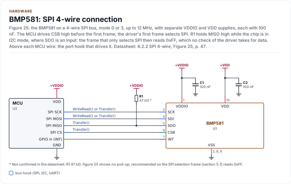
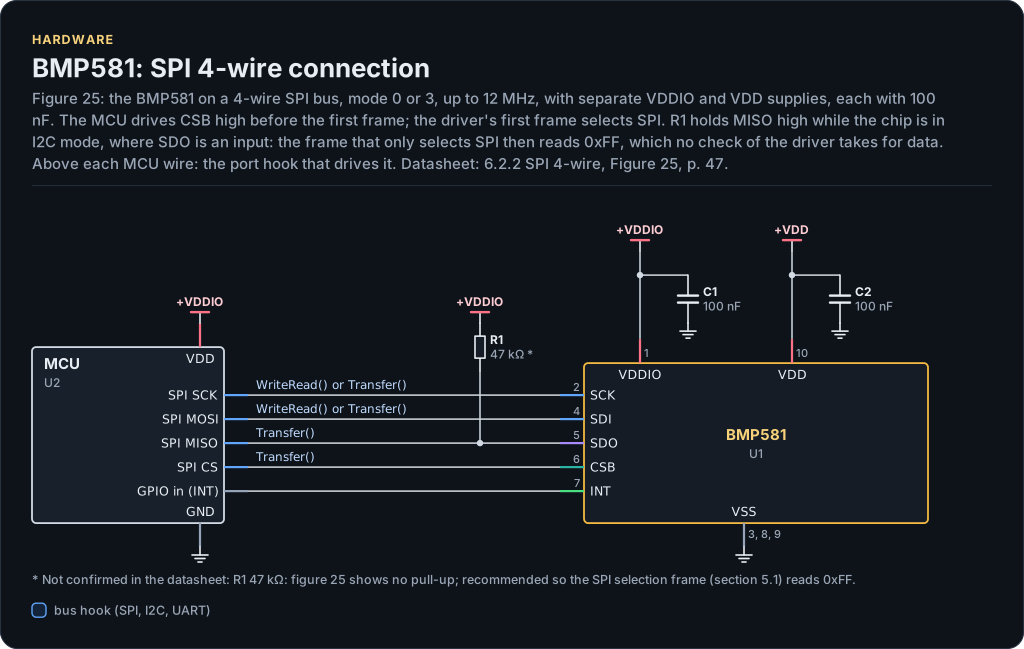
Figure description and sources
A schematic. The MCU is on the left, each of its pins level with the chip pin it connects to; above each wire is the hook of the driver's port that drives or reads it. Supply pins point up to their supply and decoupling, ground pins down. Pins on the right carry the loads and the pins tied to a supply or ground; a cross marks a pin left open. A dot is a junction; wires that cross without a dot are not connected.
Drawn from: docs/hardware.yml; inc/bmp581_i2c_interface.hpp; inc/bmp581_spi_interface.hpp.
INT pin
Push-pull or open drain, active high or low, pulsed (105 µs typical) or latched (sections 4.7.3, table 4); the
driver writes Config::int_* to INT_CONFIG and the sources to INT_SOURCE. It never reads the pin: the
application may wire it to an interrupt and then call ReadInterruptStatus() or ReadMeasurement(). Unused: tie
INT to GND and leave int_pin_enable false, its reset value (section 6.2).
Timing
| Step | Datasheet | Driver |
|---|---|---|
| Power-up to first access | t_powup ≤ 2 ms (table 4) | kPowerUpUs, waited at every start |
| Soft reset | t_soft_res ≤ 2 ms | kSoftResetUs |
| Any mode to standby | t_standby ≤ 2.5 ms | kStandbyUs, then a read that confirms it |
| Standby to a measurement | t_startup ≤ 3 ms; from deep standby 4 ms | ForcedMeasurementMaxUs() |
| Conversion | t_conv_p + t_conv_t, ±5 % (table 4) | ConversionTimeMaxUs() |
| NVM ready after reset | not given | polled, at most Config::startup_timeout_ms |
Power
| State | Current (typical, 25 °C) | How |
|---|---|---|
| Deep standby | 0.55 µA | After EnsureInitialized() with Config{}, and after Deinitialize() |
| Standby | 1.0 µA | Standby with a FIFO, an IIR filter, a data rate of 5 Hz or more, or deep_standby = false |
| Normal, 1 Hz, low power | 1.3 µA | LowPowerPreset(): deep standby between the measurements (section 4.3.5) |
| High resolution, 30 Hz | 75 µA | HighResolutionPreset() (25 Hz) |
Deep standby needs all of: deep_standby true, a data rate under 5 Hz, the FIFO off and both IIR filters
bypassed (section 4.3.2); EntersDeepStandby() says whether a configuration meets them. The driver uses the
longer start-up time (4 ms) for a forced measurement from deep standby.
Reference documents
The datasheet: BMP581 datasheet. Every pin, setting and timing on this page cites a section of it;
its revision, its SHA-256 and the sections each page relies on are in docs/datasheets.yml.
| Document | Revision | Get it |
|---|---|---|
| Datasheet: BMP581 Barometric Pressure Sensor (Bosch Sensortec BST-BMP581-DS004-13) | 1.13, 2025-04 | PDF · vendor page |
Written against these revisions; the SHA-256 of each file is in docs/datasheets.yml. Where each part
of the driver is in the datasheet: Datasheet map.