Figures
Every figure on this site is drawn by a Python module from facts extracted from the code, so it is rebuilt,
not redrawn, when the code changes. CI runs kokeb-docs figures --check and fails when a
committed figure no longer matches the code. Each figure below lists the files it is drawn from.
Inside the AT25040B
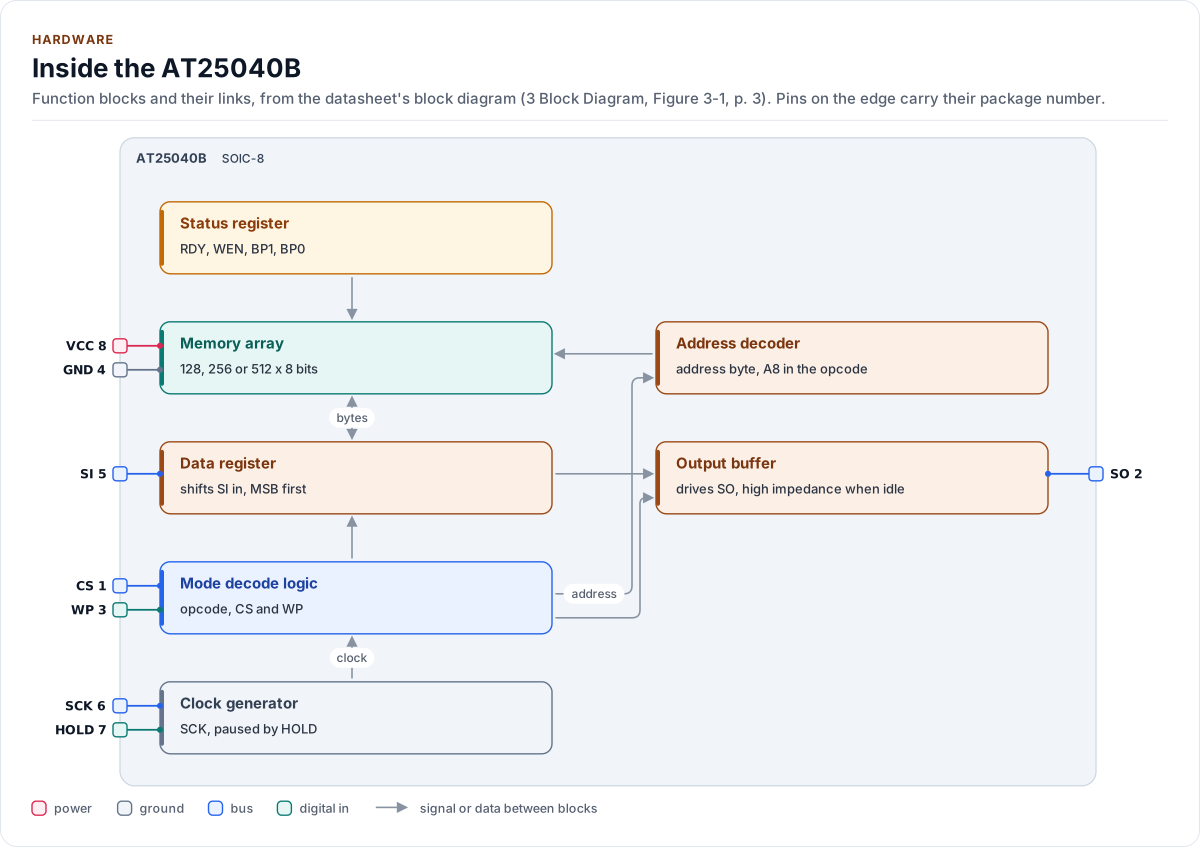
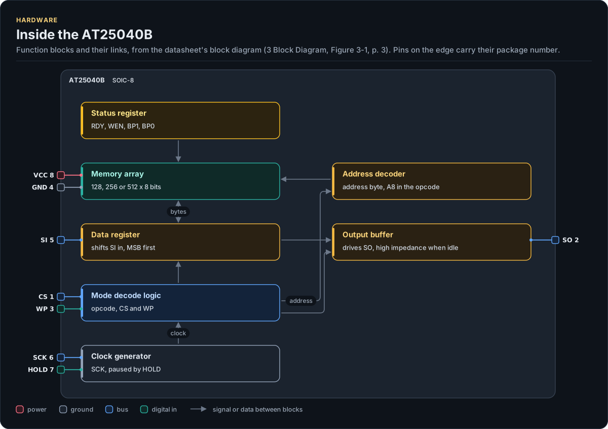
Figure description and sources
The AT25040B's function blocks inside its outline. Arrows between blocks carry signals or data in the direction they point (both ways where they have two heads). The package pins stand on the left and right edges with their numbers, each wired to the block it reaches.
Drawn from: docs/hardware.yml; inc/at25040b_spi_interface.hpp.
Hardware description: docs/hardware.yml
Drawn from:
AT25040B: Typical wiring
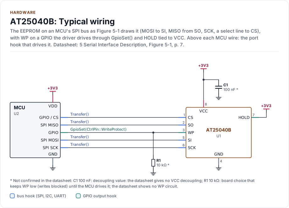
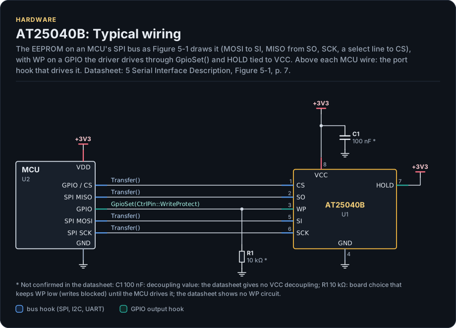
Figure description and sources
A schematic. The MCU is on the left, each of its pins level with the chip pin it connects to; above each wire is the hook of the driver's port that drives or reads it. Supply pins point up to their supply and decoupling, ground pins down. Pins on the right carry the loads and the pins tied to a supply or ground; a cross marks a pin left open. A dot is a junction; wires that cross without a dot are not connected.
Drawn from: docs/hardware.yml; inc/at25040b_spi_interface.hpp.
Hardware description: docs/hardware.yml
Drawn from:
AT25040B pinout, SOIC-8
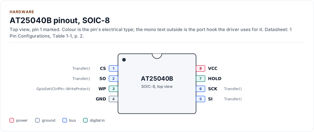
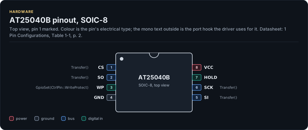
Figure description and sources
The AT25040B seen from the top, in its SOIC-8 package. Pin 1 is marked by the dot; the numbers run counter-clockwise from it. Each pad is coloured by the pin's electrical type (legend below). Next to it is the pin's name and, in mono, the hook of the driver's port that drives or reads it; a pin without a hook is not used by the driver.
Drawn from: docs/hardware.yml; inc/at25040b_spi_interface.hpp.
Hardware description: docs/hardware.yml
Drawn from:
The layers, one of them yours
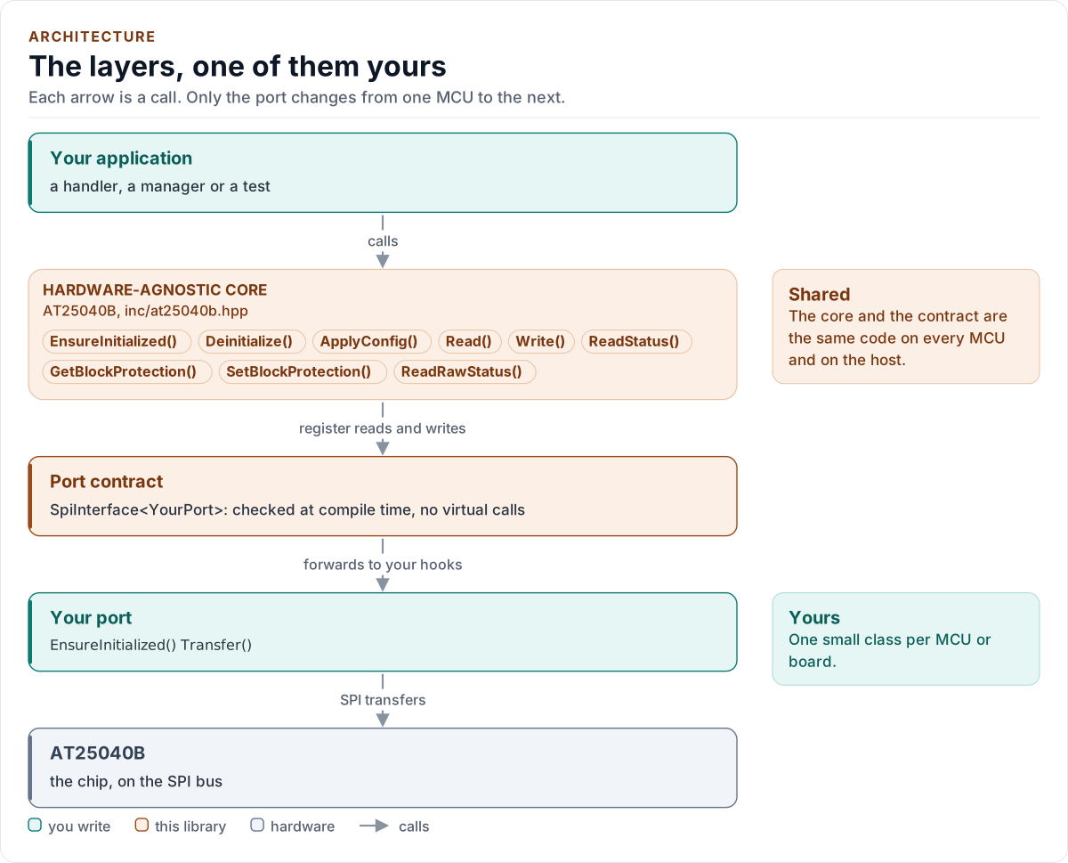
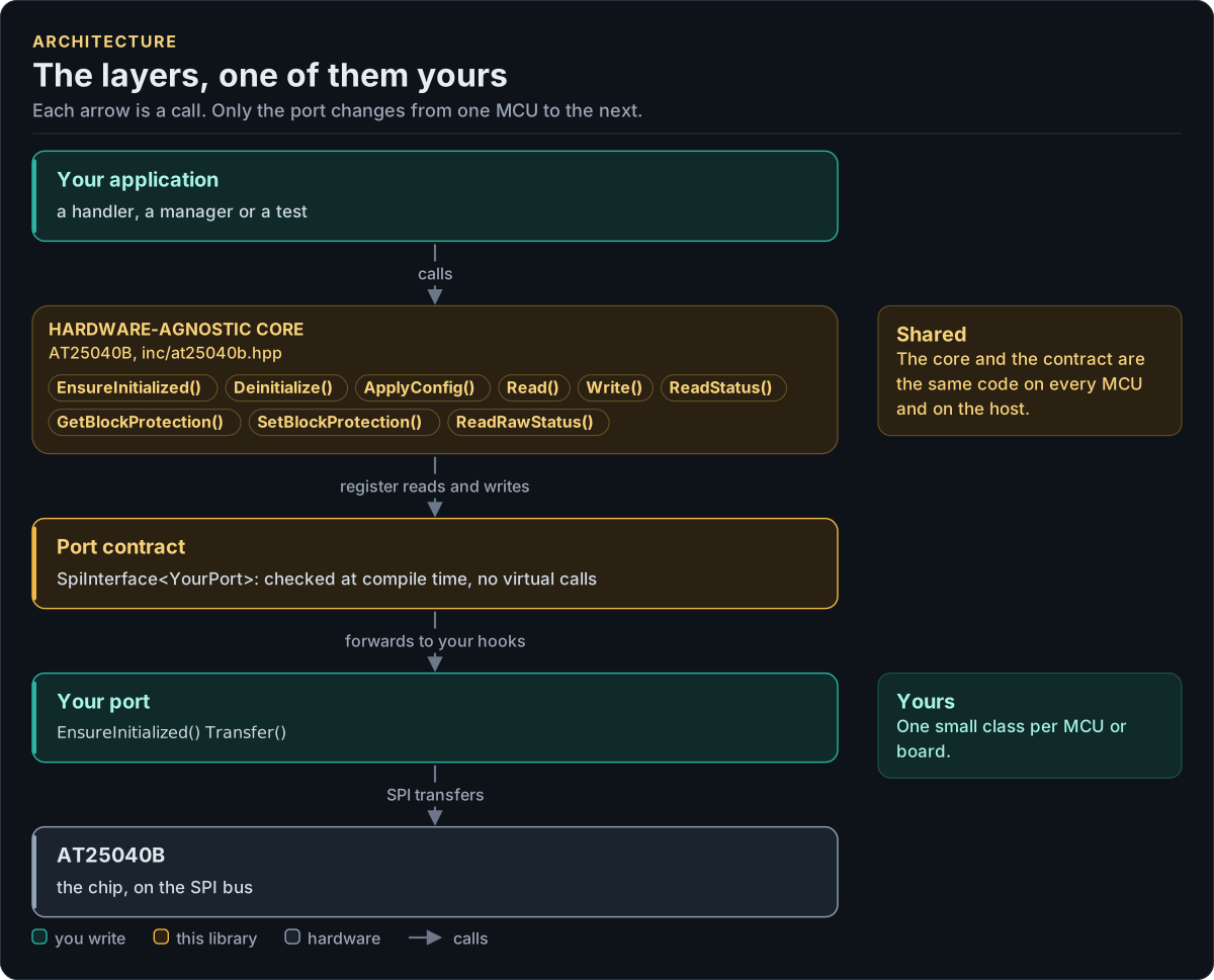
Figure description and sources
Top to bottom, each arrow is a call. Your application calls one object, whose public calls are listed from the umbrella header in inc/. The core turns each call into register reads and writes and hands them to the port contract (the CRTP base in inc/*_interface.hpp), which forwards them, at compile time, to the hooks of the port class you write; your port moves the bytes on the bus. The notes on the right say which layers stay the same on every MCU and which one you write. A library without a port contract has only the first two layers.
Drawn from: inc/at25040b.hpp public calls; inc/at25040b_spi_interface.hpp SpiInterface; figure module docs/diagrams/figures/driver-layers.py.
Figure module: docs/diagrams/figures/driver-layers.py
Drawn from:
public callsininc/at25040b.hppSpiInterfaceininc/at25040b_spi_interface.hpp
The identity check, and what a broken bus looks like
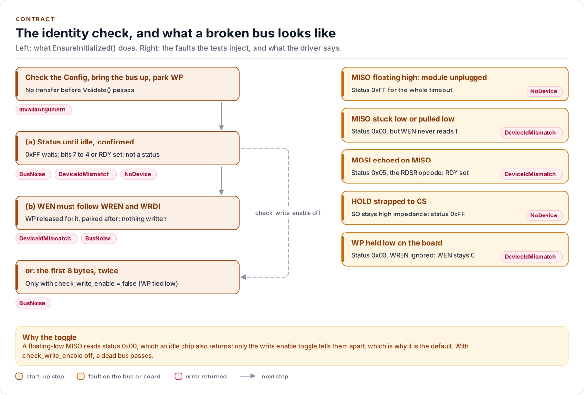
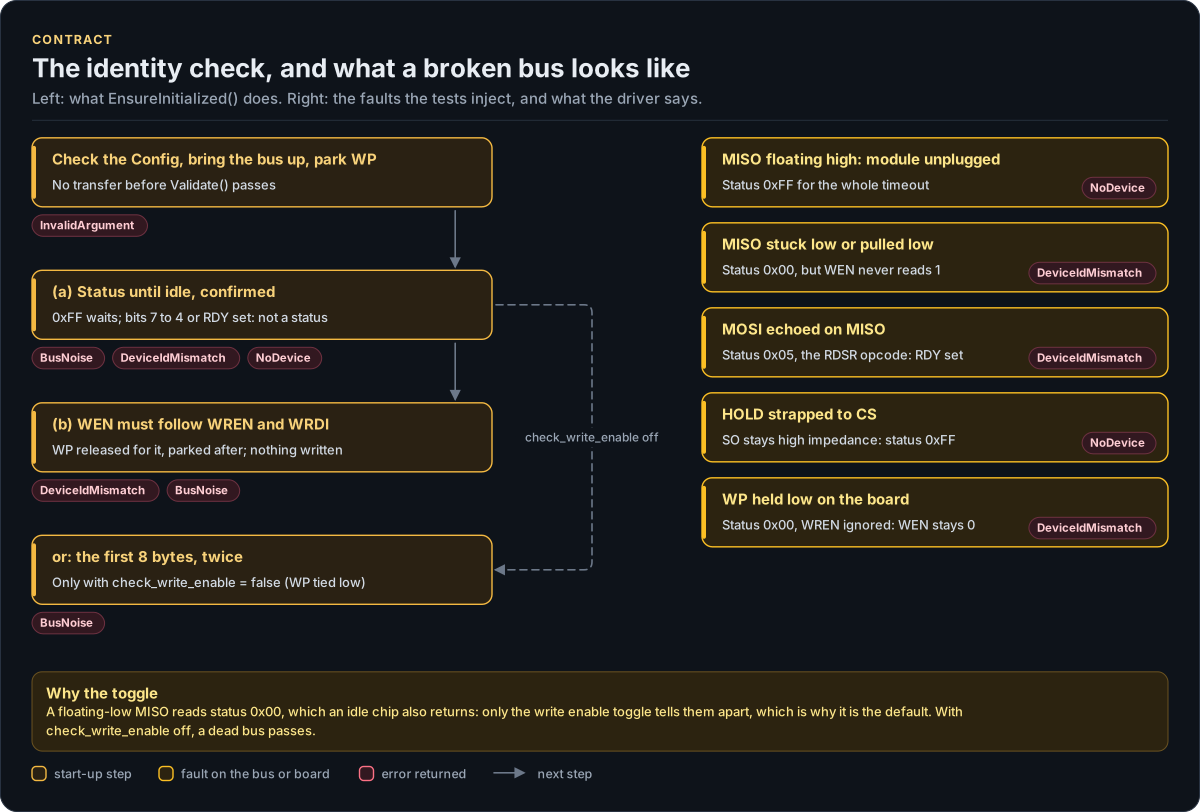
Figure description and sources
The left column is the start-up as the driver runs it, top to bottom; a pill names the error a step returns, and any step that sends a transfer also returns Bus when it fails. The status is read until it is not busy, for at most Config::write_timeout_us, and an idle status counts only when a second read gives the same byte. With Config::check_write_enable (the default) WP is released, the latch cleared first if it was set, then WREN must show WEN = 1 and WRDI WEN = 0, and WP is parked again; nothing is programmed. Without it, for a board whose WP is tied low, the first kIdentityReadBytes are read twice and must match, a weaker test. The right column lists the bus and board faults the host tests put on the chip model, each with the status byte the driver saw and the error EnsureInitialized() returned, read from the test cases in tests/test_at25040b.cpp. The steps come from initialize(), checkWriteEnableToggle(), checkStableHead() and waitIdle() in src/at25040b.ipp.
Drawn from: src/at25040b.ipp initialize; src/at25040b.ipp checkWriteEnableToggle; src/at25040b.ipp checkStableHead; src/at25040b.ipp waitIdle; tests/test_at25040b.cpp start-up fault tests; figure module docs/diagrams/figures/identity-check.py.
Figure module: docs/diagrams/figures/identity-check.py
Drawn from:
initializeinsrc/at25040b.ippcheckWriteEnableToggleinsrc/at25040b.ippcheckStableHeadinsrc/at25040b.ippwaitIdleinsrc/at25040b.ippstart-up fault testsintests/test_at25040b.cpp
Six instructions, one transfer each
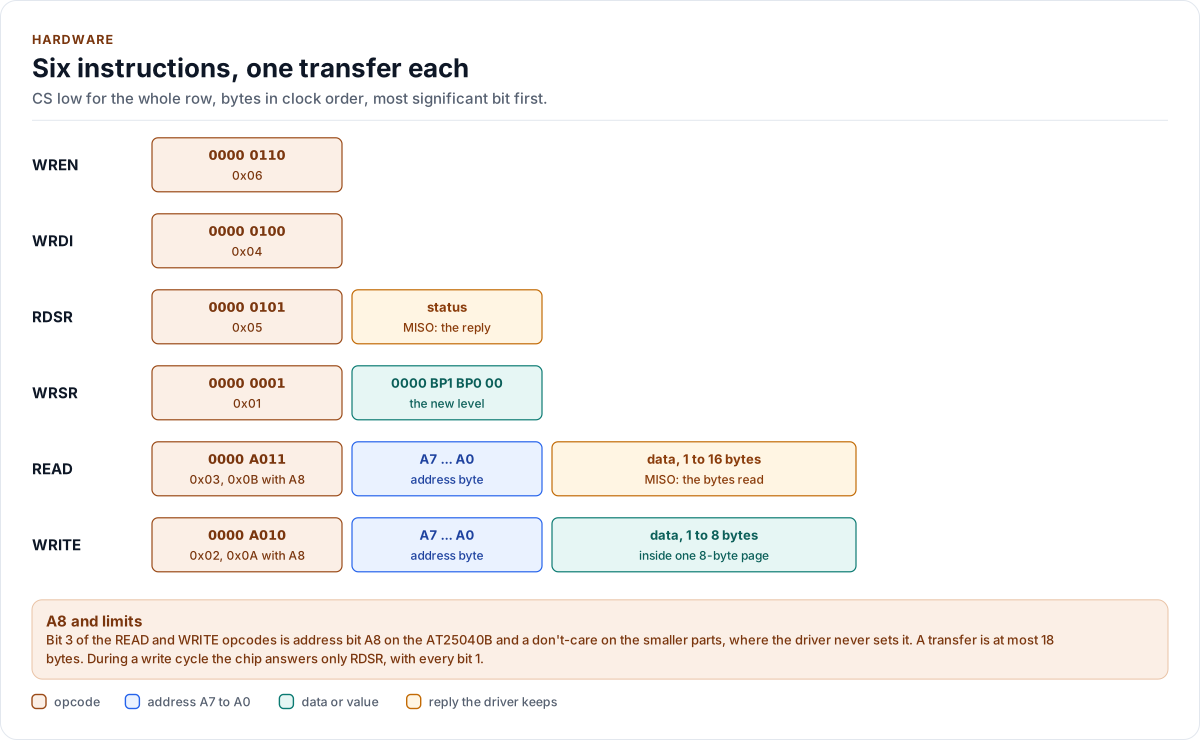
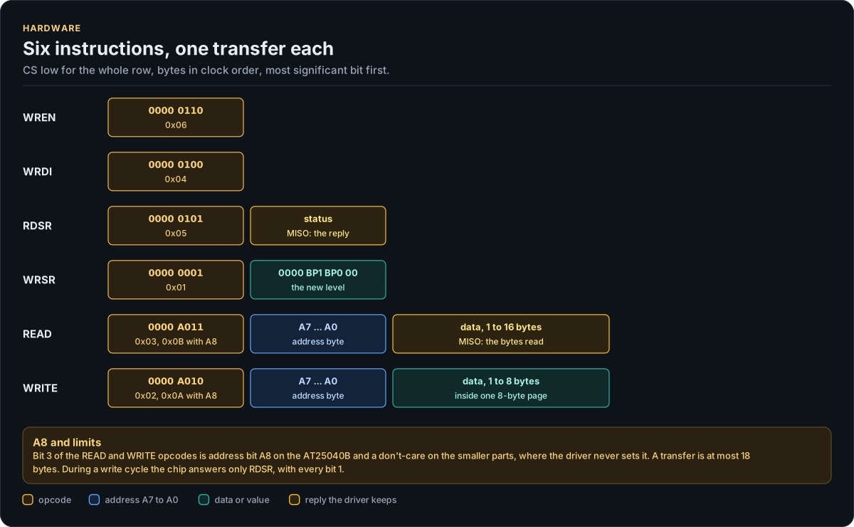
Figure description and sources
Each row is one transfer, CS low from the first byte to the last, drawn left to right in the order the bytes are clocked; the top line of a byte is what the driver sends on MOSI, the bottom line what it keeps from MISO. Every opcode is 0000 followed by four bits, written out in binary. For READ and WRITE, bit 3 of the opcode carries address bit A8 on the AT25040B and the next byte holds A7 to A0; the driver sets A8 for addresses 0x100 to 0x1FF and never on the smaller parts. RDSR returns the status in its second byte; READ returns data from the third byte on, up to kReadChunkBytes per transfer; WRITE carries 1 to kPageSizeBytes data bytes inside one page. WREN, WRDI, WRSR and WRITE need no reply, and the driver passes no receive buffer for them. The opcodes come from inc/at25040b_registers.hpp and the byte layouts from detail::EepromBus in inc/at25040b_spi_interface.hpp.
Drawn from: inc/at25040b_registers.hpp opcodes; inc/at25040b_spi_interface.hpp detail::EepromBus; inc/at25040b_types.hpp kReadChunkBytes; figure module docs/diagrams/figures/instruction-frames.py.
Figure module: docs/diagrams/figures/instruction-frames.py
Drawn from:
opcodesininc/at25040b_registers.hppdetail::EepromBusininc/at25040b_spi_interface.hppkReadChunkBytesininc/at25040b_types.hpp
Write(), step by step
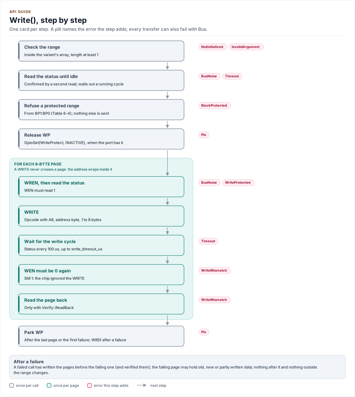
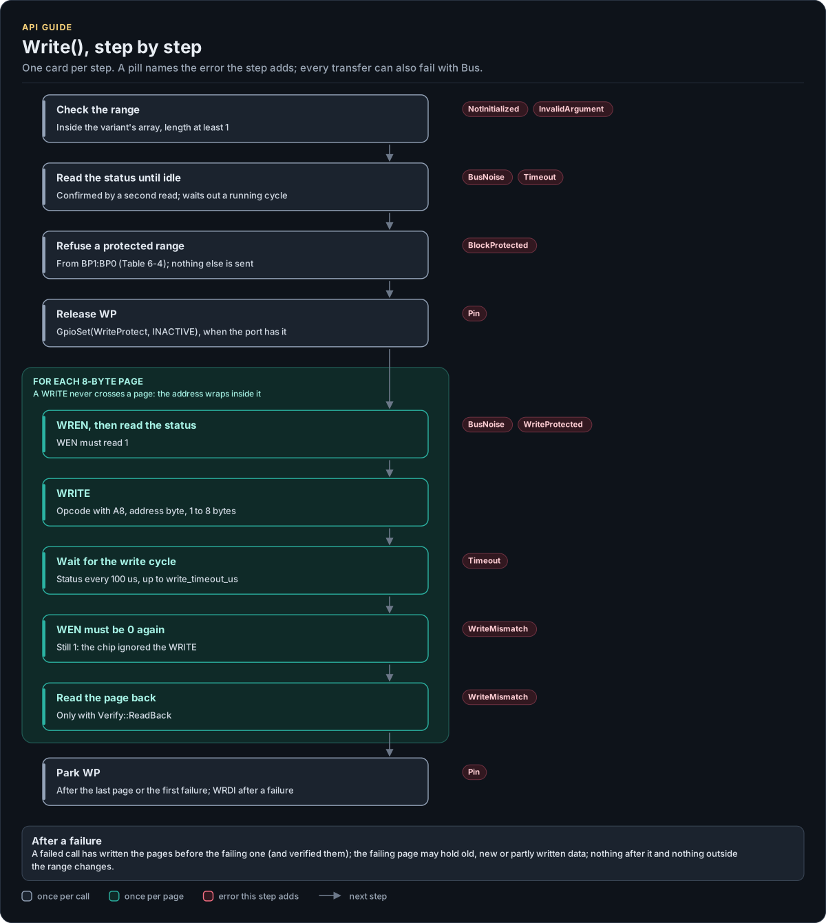
Figure description and sources
Top to bottom, one card per step of Write(); a pill on a card names the error that step can return, and any step that sends a transfer also returns Bus when the transfer fails. The first two steps read the status (until no write cycle runs, confirmed by a second read) and refuse a range that overlaps the block-protected part before anything else is sent. WP is then released, if the port drives it. The band in the middle repeats once per 8-byte page: WREN and a status read that must show WEN = 1, the WRITE, a wait for the write cycle polled every kPollIntervalUs up to Config::write_timeout_us, a status that must show WEN = 0 again (still 1 means the chip ignored the WRITE), and only when the call passes Verify::ReadBack a read-back of the page. After the last page, or the first failure, WP is parked; a failure after WREN also sends WRDI. The steps and errors are read from writeRange(), writePage(), enableWrite(), finishWriteCycle(), waitIdle() and withWriteAccess() in src/at25040b.ipp.
Drawn from: src/at25040b.ipp Write; src/at25040b.ipp writeRange; src/at25040b.ipp writePage; src/at25040b.ipp enableWrite; src/at25040b.ipp finishWriteCycle; src/at25040b.ipp waitIdle; src/at25040b.ipp withWriteAccess; figure module docs/diagrams/figures/write-path.py.
Figure module: docs/diagrams/figures/write-path.py
Drawn from:
Writeinsrc/at25040b.ippwriteRangeinsrc/at25040b.ippwritePageinsrc/at25040b.ippenableWriteinsrc/at25040b.ippfinishWriteCycleinsrc/at25040b.ippwaitIdleinsrc/at25040b.ippwithWriteAccessinsrc/at25040b.ipp