Hardware
The ADS9324's pins, supplies, reference, bus settings and timing, as the driver uses them.
Datasheet sections this page relies on
From Texas Instruments SBASB22 -:
- Features, channel count and the 16 simultaneous samples: 1 Features; 3 Description, p. 1
- Pins, package and the data lanes: 4 Pin Configuration and Functions, p. 3
- Absolute maximum ratings: 5.1 Absolute Maximum Ratings, p. 5
- Supplies, reference and input ranges: 5.3 Recommended Operating Conditions, p. 6
- Electrical characteristics, power-up and reset times: 5.5 Electrical Characteristics, p. 7
- SPI and CONVST timing: 5.6 Timing Requirements; 5.7 Switching Characteristics, p. 11
- Analog inputs and the input clamps: 7.3.1 Analog Inputs; 7.3.2 Input Clamp Protection Circuit, p. 25
- Reference selection: 7.3.6 Reference, Table 7-3, p. 28
- Alarm modes and the DRDY/ALARM pin: 7.3.13 Alarm Modes, Table 7-10, p. 41
- Reset: 7.4.1 Reset, p. 49
- Typical application and input filter: 9.2 Typical Application, Figures 9-1 and 9-2, p. 106
- Power-supply decoupling: 9.3 Power Supply Recommendations, Figure 9-4, p. 109
- Layout: 9.4 Layout, p. 109
- Package outline and ordering: 12 Mechanical, Packaging, and Orderable Information, p. 112
All of them, with the driver API for each: Datasheet map.
The ADS9324 is a 16-channel, 16-bit, simultaneous-sampling SAR ADC. Each channel has its own clamp, programmable gain amplifier (1 MΩ input impedance) and ADC; one CONVST edge samples all 16 channels together. The registers are read and written over SPI; the conversion results come out on SDOUT (one lane) or on the D0 to D7 pins (2, 4 or 8 lanes). The driver works with the one package the datasheet lists, the 64-pin VQFN (RSK).
Pins
The pinout, the block diagram, the circuit and the two tables on this page are drawn from
docs/hardware.yml.
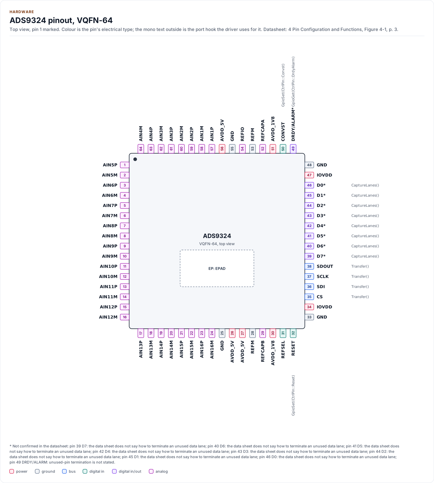
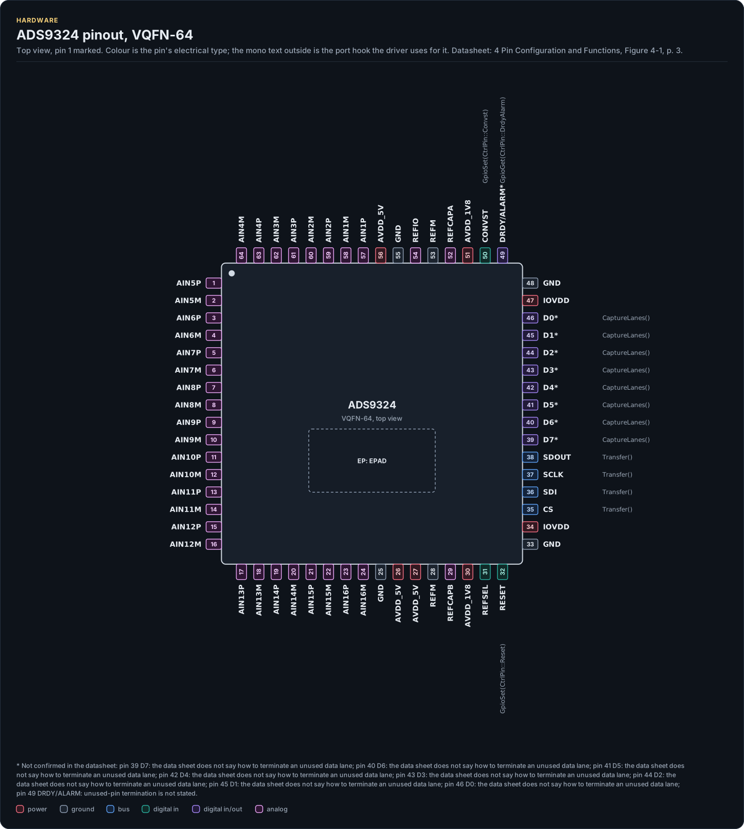
Figure description and sources
The ADS9324 seen from the top, in its VQFN-64 package. Pin 1 is marked by the dot; the numbers run counter-clockwise from it. Each pad is coloured by the pin's electrical type (legend below). Next to it is the pin's name and, in mono, the hook of the driver's port that drives or reads it; a pin without a hook is not used by the driver. The dashed square is the exposed pad.
Drawn from: docs/hardware.yml; inc/ads9324.hpp; inc/ads9324_spi_interface.hpp.
VQFN-64, 64 pins and an exposed pad (4 Pin Configuration and Functions, Figure 4-1, p. 3).
| Pin | Name | Type (domain) | Function | Driver hook | If unused | Datasheet |
|---|---|---|---|---|---|---|
| 1 | AIN5P |
analog (AVDD_5V) | Analog input channel 5, positive input | - | - | 4, p. 3 |
| 2 | AIN5M |
analog (AVDD_5V) | Analog input channel 5, negative input | - | - | 4, p. 3 |
| 3 | AIN6P |
analog (AVDD_5V) | Analog input channel 6, positive input | - | - | 4, p. 3 |
| 4 | AIN6M |
analog (AVDD_5V) | Analog input channel 6, negative input | - | - | 4, p. 3 |
| 5 | AIN7P |
analog (AVDD_5V) | Analog input channel 7, positive input | - | - | 4, p. 3 |
| 6 | AIN7M |
analog (AVDD_5V) | Analog input channel 7, negative input | - | - | 4, p. 3 |
| 7 | AIN8P |
analog (AVDD_5V) | Analog input channel 8, positive input | - | - | 4, p. 3 |
| 8 | AIN8M |
analog (AVDD_5V) | Analog input channel 8, negative input | - | - | 4, p. 3 |
| 9 | AIN9P |
analog (AVDD_5V) | Analog input channel 9, positive input | - | - | 4, p. 3 |
| 10 | AIN9M |
analog (AVDD_5V) | Analog input channel 9, negative input | - | - | 4, p. 3 |
| 11 | AIN10P |
analog (AVDD_5V) | Analog input channel 10, positive input | - | - | 4, p. 3 |
| 12 | AIN10M |
analog (AVDD_5V) | Analog input channel 10, negative input | - | - | 4, p. 3 |
| 13 | AIN11P |
analog (AVDD_5V) | Analog input channel 11, positive input | - | - | 4, p. 3 |
| 14 | AIN11M |
analog (AVDD_5V) | Analog input channel 11, negative input | - | - | 4, p. 3 |
| 15 | AIN12P |
analog (AVDD_5V) | Analog input channel 12, positive input | - | - | 4, p. 3 |
| 16 | AIN12M |
analog (AVDD_5V) | Analog input channel 12, negative input | - | - | 4, p. 3 |
| 17 | AIN13P |
analog (AVDD_5V) | Analog input channel 13, positive input | - | - | 4, p. 3 |
| 18 | AIN13M |
analog (AVDD_5V) | Analog input channel 13, negative input | - | - | 4, p. 3 |
| 19 | AIN14P |
analog (AVDD_5V) | Analog input channel 14, positive input | - | - | 4, p. 3 |
| 20 | AIN14M |
analog (AVDD_5V) | Analog input channel 14, negative input | - | - | 4, p. 3 |
| 21 | AIN15P |
analog (AVDD_5V) | Analog input channel 15, positive input | - | - | 4, p. 3 |
| 22 | AIN15M |
analog (AVDD_5V) | Analog input channel 15, negative input | - | - | 4, p. 3 |
| 23 | AIN16P |
analog (AVDD_5V) | Analog input channel 16, positive input | - | - | 4, p. 3 |
| 24 | AIN16M |
analog (AVDD_5V) | Analog input channel 16, negative input | - | - | 4, p. 3 |
| 25 | GND |
ground | Ground | - | - | 4, p. 4 |
| 26 | AVDD_5V |
power (AVDD_5V) | 5 V analog supply, 4.75 V to 5.25 V; 1 µF and 0.1 µF to GND at each supply pin | - | - | 9.3, p. 109 |
| 27 | AVDD_5V |
power (AVDD_5V) | 5 V analog supply, 4.75 V to 5.25 V; 1 µF and 0.1 µF to GND at each supply pin | - | - | 9.3, p. 109 |
| 28 | REFM |
ground | Reference ground; short to the GND plane outside the device | - | - | 4, p. 4 |
| 29 | REFCAPB |
analog (AVDD_5V) | Reference amplifier output; 1 µF low-ESR X7R to REFM (pin 28) | - | - | 4, p. 4 |
| 30 | AVDD_1V8 |
power (AVDD_1V8) | 1.8 V supply, 1.7 V to 1.9 V; 1 µF and 0.1 µF to GND at each supply pin | - | - | 9.3, p. 109 |
| 31 | REFSEL |
digital in (IOVDD) | Reference source: high selects the internal reference, low the external one (Table 7-3) | - | - | 7.3.6, p. 28 |
| 32 | RESET |
digital in (IOVDD) | Hardware reset, active low | GpioSet(CtrlPin::Reset) |
- | 4, p. 4 |
| 33 | GND |
ground | Ground | - | - | 4, p. 4 |
| 34 | IOVDD |
power (IOVDD) | Digital I/O supply, 1.7 V to 3.6 V; 1 µF and 0.1 µF to GND at each supply pin | - | - | 9.3, p. 109 |
| 35 | CS |
bus (IOVDD) | SPI chip select, active low | Transfer() |
- | 4, p. 4 |
| 36 | SDI |
bus (IOVDD) | SPI data in (MOSI) | Transfer() |
- | 4, p. 4 |
| 37 | SCLK |
bus (IOVDD) | SPI clock, up to 60 MHz | Transfer() |
- | 4, p. 4 |
| 38 | SDOUT |
bus (IOVDD) | SPI data out (MISO): register replies and the data of the 1-lane mode | Transfer() |
- | 4, p. 4 |
| 39 | D7 1 |
digital in/out (IOVDD) | Serial output data lane 7 | CaptureLanes() |
Leave open | 4, p. 4 |
| 40 | D6 2 |
digital in/out (IOVDD) | Serial output data lane 6 | CaptureLanes() |
Leave open | 4, p. 4 |
| 41 | D5 3 |
digital in/out (IOVDD) | Serial output data lane 5 | CaptureLanes() |
Leave open | 4, p. 4 |
| 42 | D4 4 |
digital in/out (IOVDD) | Serial output data lane 4 | CaptureLanes() |
Leave open | 4, p. 4 |
| 43 | D3 5 |
digital in/out (IOVDD) | Serial output data lane 3 or daisy-chain input 3 | CaptureLanes() |
Leave open | 4, p. 4 |
| 44 | D2 6 |
digital in/out (IOVDD) | Serial output data lane 2 or daisy-chain input 2 | CaptureLanes() |
Leave open | 4, p. 4 |
| 45 | D1 7 |
digital in/out (IOVDD) | Serial output data lane 1 or daisy-chain input 1 | CaptureLanes() |
Leave open | 4, p. 4 |
| 46 | D0 8 |
digital in/out (IOVDD) | Serial output data lane 0 or daisy-chain input 0 | CaptureLanes() |
Leave open | 4, p. 4 |
| 47 | IOVDD |
power (IOVDD) | Digital I/O supply, 1.7 V to 3.6 V; 1 µF and 0.1 µF to GND at each supply pin | - | - | 9.3, p. 109 |
| 48 | GND |
ground | Ground | - | - | 4, p. 4 |
| 49 | DRDY/ALARM 9 |
digital in/out (IOVDD) | Data ready or alarm, active high; polarity and source in DRDY_ALARM_SEL | GpioGet(CtrlPin::DrdyAlarm) |
Leave open | 4, p. 4 |
| 50 | CONVST |
digital in (IOVDD) | Start of conversion: the falling edge samples all 16 channels (section 7.4.2); keep it high before DRDY rises in the internal oversampling mode (Figure 5-7) | GpioSet(CtrlPin::Convst) |
- | 4, p. 4 |
| 51 | AVDD_1V8 |
power (AVDD_1V8) | 1.8 V supply, 1.7 V to 1.9 V; 1 µF and 0.1 µF to GND at each supply pin | - | - | 9.3, p. 109 |
| 52 | REFCAPA |
analog (AVDD_5V) | Reference amplifier output; 1 µF low-ESR X7R to REFM (pin 53) | - | - | 4, p. 4 |
| 53 | REFM |
ground | Reference ground; short to the GND plane outside the device | - | - | 4, p. 4 |
| 54 | REFIO |
analog (AVDD_5V) | Internal reference output (REFSEL high) or external reference input (REFSEL low); 4.7 µF to REFM | - | - | 4, p. 4 |
| 55 | GND |
ground | Ground | - | - | 4, p. 4 |
| 56 | AVDD_5V |
power (AVDD_5V) | 5 V analog supply, 4.75 V to 5.25 V; 1 µF and 0.1 µF to GND at each supply pin | - | - | 9.3, p. 109 |
| 57 | AIN1P |
analog (AVDD_5V) | Analog input channel 1, positive input | - | - | 4, p. 3 |
| 58 | AIN1M |
analog (AVDD_5V) | Analog input channel 1, negative input | - | - | 4, p. 3 |
| 59 | AIN2P |
analog (AVDD_5V) | Analog input channel 2, positive input | - | - | 4, p. 3 |
| 60 | AIN2M |
analog (AVDD_5V) | Analog input channel 2, negative input | - | - | 4, p. 3 |
| 61 | AIN3P |
analog (AVDD_5V) | Analog input channel 3, positive input | - | - | 4, p. 3 |
| 62 | AIN3M |
analog (AVDD_5V) | Analog input channel 3, negative input | - | - | 4, p. 3 |
| 63 | AIN4P |
analog (AVDD_5V) | Analog input channel 4, positive input | - | - | 4, p. 3 |
| 64 | AIN4M |
analog (AVDD_5V) | Analog input channel 4, negative input | - | - | 4, p. 3 |
| EP | EPAD |
ground | Exposed thermal pad; connect to GND | - | - | 4, p. 4 |
Source of this table and of the chip figures: docs/hardware.yml.
The package outline, drawn to scale:
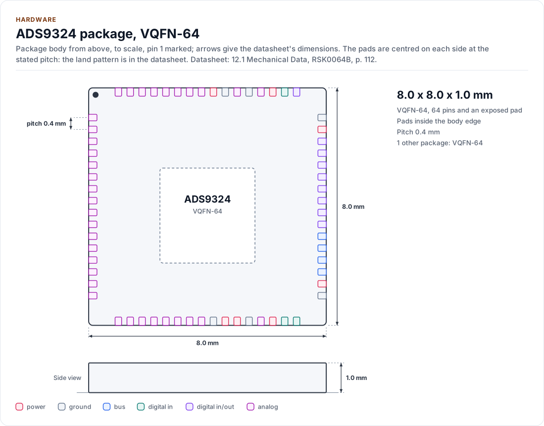
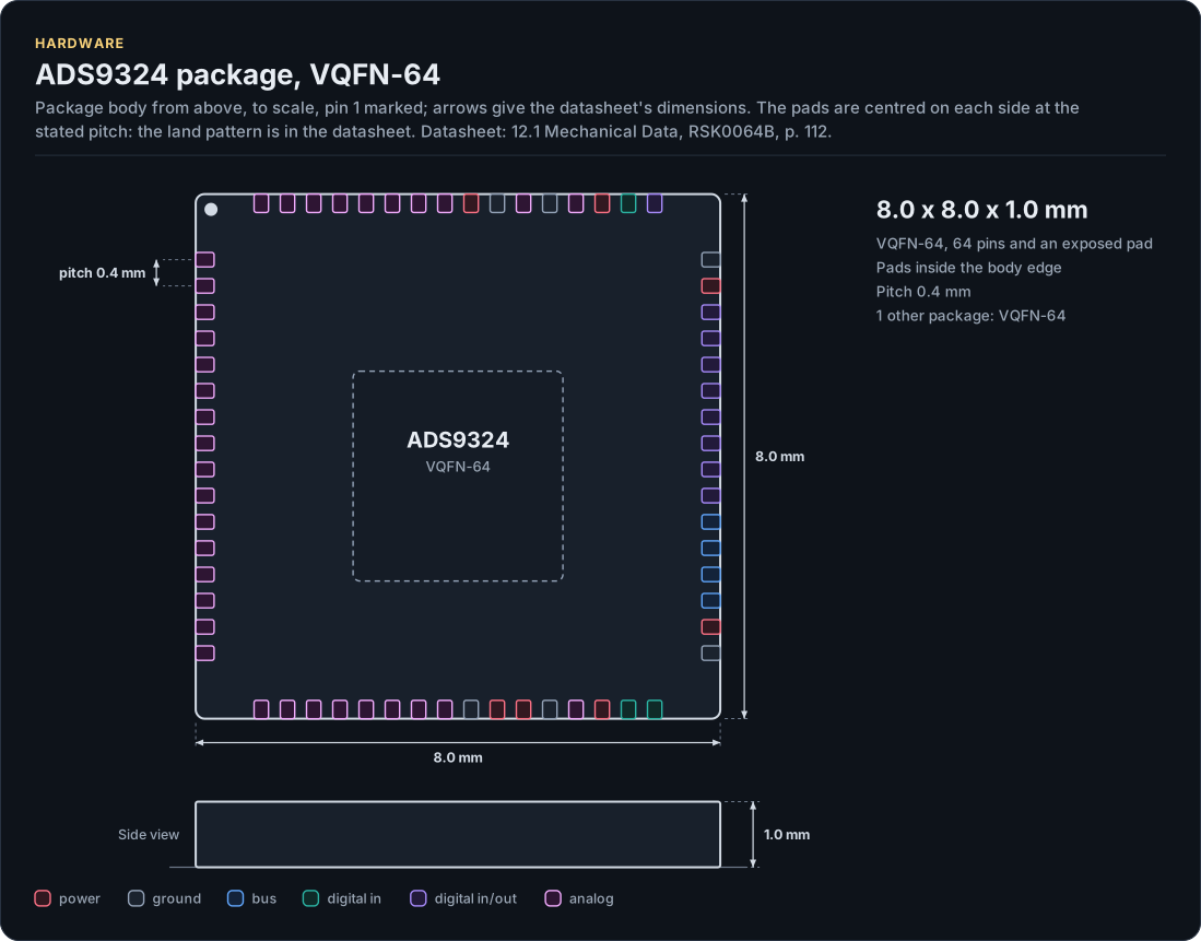
Figure description and sources
The ADS9324 package seen from the top and, when the height is known, from the side, drawn to scale: 8.0 x 8.0 x 1.0 mm. The arrows carry the datasheet's dimensions, the dot marks pin 1 and the pads are numbered counter-clockwise from it, coloured by the pin's electrical type (legend below). Pads sit centred on each side at the stated pitch; the datasheet's land pattern is the reference for a board.
Drawn from: docs/hardware.yml; inc/ads9324.hpp; inc/ads9324_spi_interface.hpp.
Inside the chip
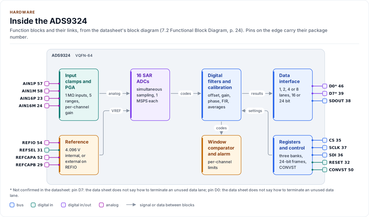
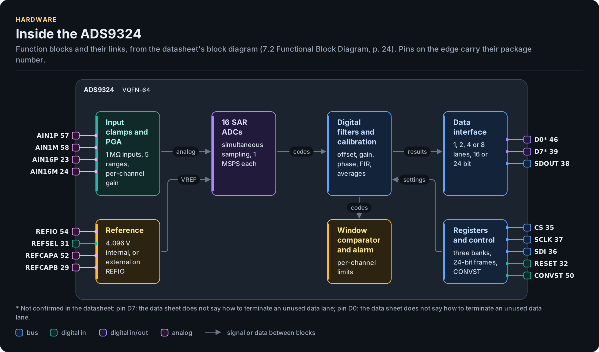
Figure description and sources
The ADS9324's function blocks inside its outline. Arrows between blocks carry signals or data in the direction they point (both ways where they have two heads). The package pins stand on the left and right edges with their numbers, each wired to the block it reaches.
Drawn from: docs/hardware.yml; inc/ads9324.hpp; inc/ads9324_spi_interface.hpp.
Typical application
One channel with the internal reference (REFSEL high), the data on SDOUT and the three supplies decoupled as Figure 9-4 shows. The other fifteen channels repeat the input filter of the first. The series resistors and the capacitor of the filter are values you choose: the datasheet gives the matched topology (Figure 9-2) and says to match the source resistance on both inputs, not a value.
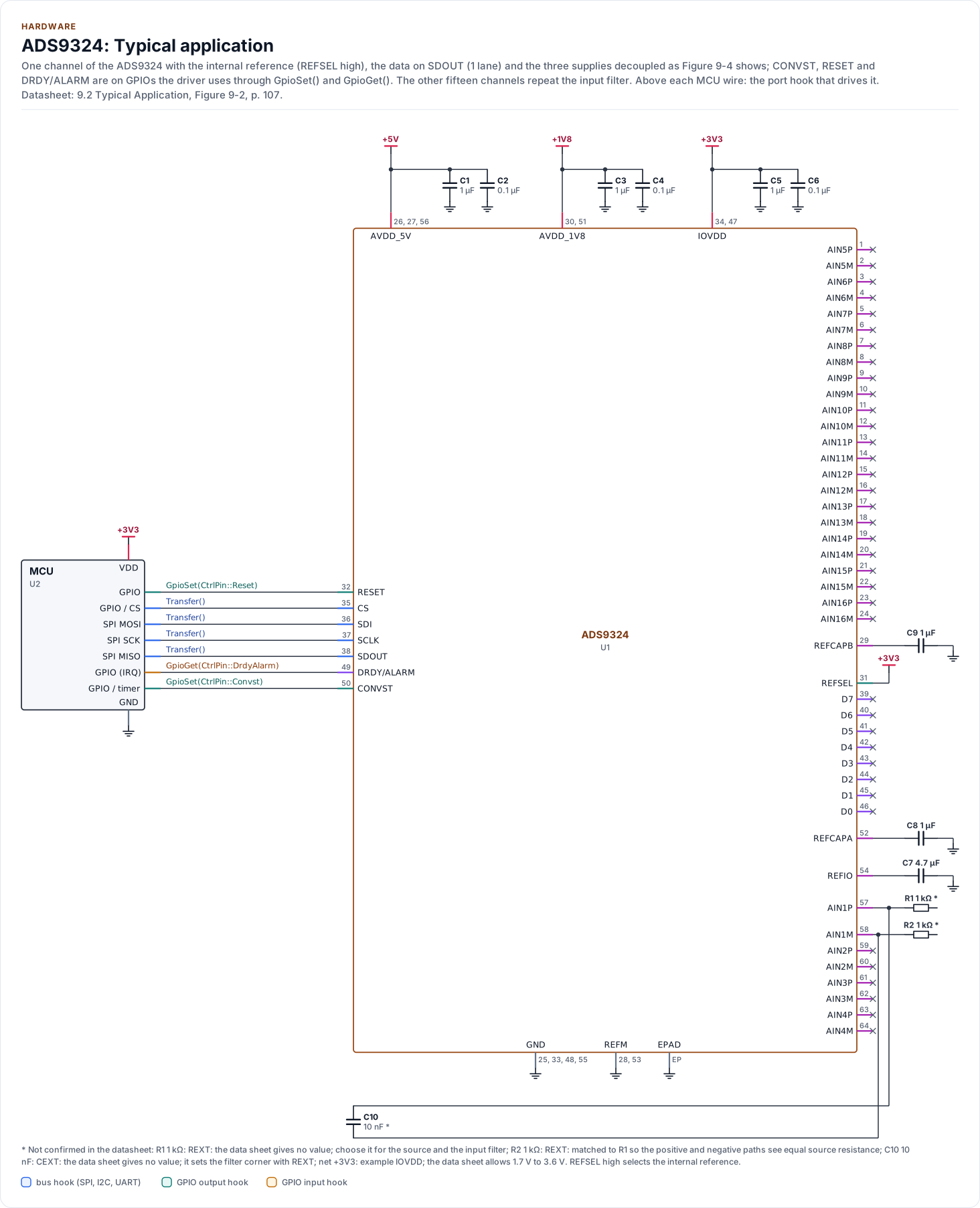
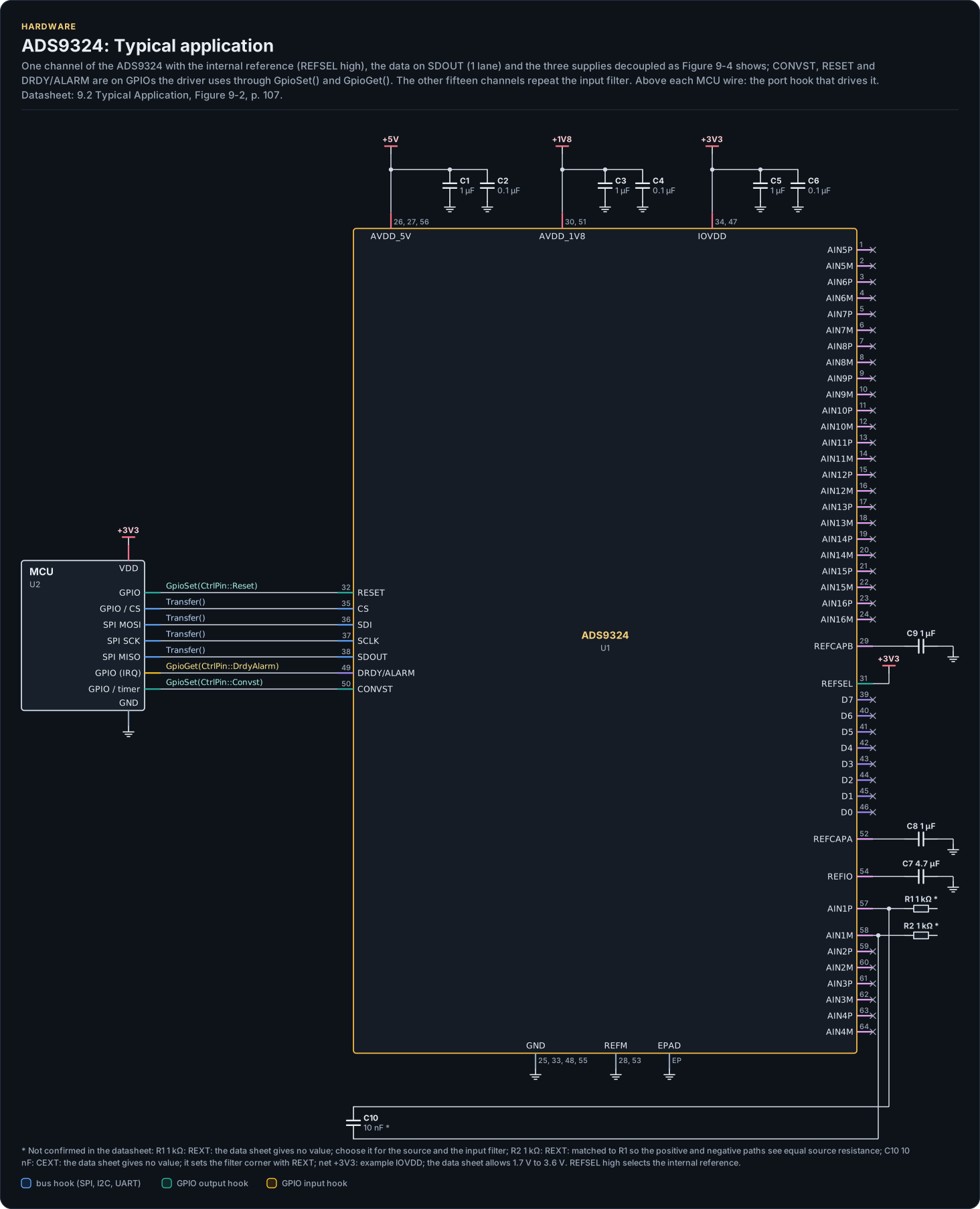
Figure description and sources
A schematic. The MCU is on the left, each of its pins level with the chip pin it connects to; above each wire is the hook of the driver's port that drives or reads it. Supply pins point up to their supply and decoupling, ground pins down. Pins on the right carry the loads and the pins tied to a supply or ground; a cross marks a pin left open. A dot is a junction; wires that cross without a dot are not connected.
Drawn from: docs/hardware.yml; inc/ads9324.hpp; inc/ads9324_spi_interface.hpp.
| Part | Kind | Value | Connects | Datasheet |
|---|---|---|---|---|
| U2 | MCU | - | VDD: +3V3, GND: GND, SCK: SCLK, MOSI: SDI, MISO: SDOUT, CS: CS, RST: RESET, CNV: CONVST, RDY: DRDY | 9.2, p. 107 |
| C1 | capacitor | 1 µF | +5V, GND | 9.3, p. 109 |
| C2 | capacitor | 0.1 µF | +5V, GND | 9.3, p. 109 |
| C3 | capacitor | 1 µF | +1V8, GND | 9.3, p. 109 |
| C4 | capacitor | 0.1 µF | +1V8, GND | 9.3, p. 109 |
| C5 | capacitor | 1 µF | +3V3, GND | 9.3, p. 109 |
| C6 | capacitor | 0.1 µF | +3V3, GND | 9.3, p. 109 |
| C7 | capacitor | 4.7 µF | GND, REFIO | 4, p. 4 |
| C8 | capacitor | 1 µF | GND, REFCAPA | 4, p. 4 |
| C9 | capacitor | 1 µF | GND, REFCAPB | 4, p. 4 |
| R1 | resistor | 1 kΩ (not confirmed: REXT: the data sheet gives no value; choose it for the source and the input filter) | IN1P | 9.2, p. 107 |
| R2 | resistor | 1 kΩ (not confirmed: REXT: matched to R1 so the positive and negative paths see equal source resistance) | IN1M | 9.2, p. 107 |
| C10 | capacitor | 10 nF (not confirmed: CEXT: the data sheet gives no value; it sets the filter corner with REXT) | IN1P, IN1M | 9.2, p. 107 |
Export a circuit for a schematic or PCB tool: kokeb-docs hardware --kicad-netlist OUT.net --circuit typical.
Export the circuit for a schematic or PCB tool: kokeb-docs hardware --kicad-netlist OUT.net --circuit typical.
Supplies
| Rail | Pins | Range | At each pin |
|---|---|---|---|
| AVDD_5V | 26, 27, 56 | 4.75 V to 5.25 V | 1 µF and 0.1 µF to GND |
| AVDD_1V8 | 30, 51 | 1.7 V to 1.9 V | 1 µF and 0.1 µF to GND |
| IOVDD | 34, 47 | 1.7 V to 3.6 V (the data timing is specified at 1.7 V to 1.9 V) | 1 µF and 0.1 µF to GND |
There is no required power-up order. With a 1.8 V IOVDD, AVDD_1V8 may be tied to IOVDD through a 100 Ω ferrite
bead (section 9.3). Config::supply takes the rails in millivolts so Validate() can reject a value outside these
ranges; leave a rail at 0 when you do not want it checked. The absolute maximum ratings (section 5.1) are
documentation only: AIN pins to ±18 V, input current 10 mA, so a series resistor on every input is required
when a source can exceed the rating.
Reference
ReferenceSource |
REFSEL pin | Result |
|---|---|---|
Pin (reset value) |
high | Internal 4.096 V reference |
Pin |
low | External reference on REFIO |
Internal |
ignored | Internal reference |
External |
ignored | External reference on REFIO |
REFIO takes 4.7 µF to REFM; REFCAPA and REFCAPB each take 1 µF (low ESR, X7R) to REFM. With the external source
the reference must be 4.096 V (4.086 V to 4.106 V). SetReference() waits 30 ms for the reference to settle.
The driver never drives REFSEL: tie it, or let Pin follow the board.
Control pins
Each control pin has a defined idle level, and the port drives it there before it enables the pin's output and before the driver's first transfer (handbook KB-HW-018): configuring a pin as an output first and setting its level afterwards gives the chip a pulse it did not ask for, a reset or a conversion.
CtrlPin |
Package pin | Polarity | Idle level | Hook |
|---|---|---|---|---|
Reset |
RESET (32) | active low | high (INACTIVE) |
GpioSet() |
Convst |
CONVST (50) | the falling edge samples; ACTIVE is high |
high (ACTIVE) |
GpioSet() |
DrdyAlarm |
DRDY/ALARM (49) | active high; Alarm::active_low inverts it |
an input | GpioGet() |
A pin tied on the board needs no hook: RESET tied high leaves Reset(ResetKind::Hardware) returning
Error::Unsupported, and a CONVST driven by a timer is used with ReadFrame() instead of MeasureOnce().
Bus settings
| Setting | Value |
|---|---|
| SPI mode | 0 (CPOL = 0, CPHA = 0); the datasheet names none, mode 0 follows its timing diagram (assumption A1) |
| Clock | Up to 60 MHz for writes (kMaxClockHz); up to 29 MHz when SDOUT is read (kMaxSdoutClockHz): above it the 17 ns SDOUT delay no longer fits half a period in mode 0 |
| Bit order | MSB first |
| Register frame | 24 bits: 8 address bits, then 16 data bits; CS low for the whole frame |
| Register read | Select the bank (BANK_SEL), write GEN_CFG1 with the address and the read bit, then clock one frame of zeros: the reply carries the data |
| Data frame | 16 or 24 bits per channel, up to 16 channels, plus an optional DIAG byte and a PRBS byte: at most 50 bytes |
| Chip select | kMinCsHighNs (16 ns) high between frames; one transfer per frame |
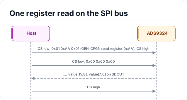
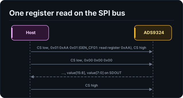
Figure description and sources
Participants, left to right: Host and ADS9324. The steps run from top to bottom. Host sends CS low, 0x01 0xAA 0x01 (GEN_CFG1: read register 0xAA), CS high to ADS9324. Host sends CS low, 0x00 0x00 0x00 to ADS9324. ADS9324 returns ..., value[15:8], value[7:0] on SDOUT to Host. Host sends CS high to ADS9324.
Drawn from: docs/model/spi-register-read.seq.yml.
On a data readout the driver always sends zeros, so no register is written by accident while the data is clocked out (assumption A9).
Timing
| Parameter | Value | Driver |
|---|---|---|
| Power-up to the first access | 30 ms | kPowerUpMs: waited by EnsureInitialized() before the first frame |
| Reset | 30 ms | kResetMs: waited after a software or hardware reset |
| RESET low pulse | 1 ms | kResetPulseUs: the datasheet gives none, so a long pulse is a design choice |
| CONVST frequency | 100 kHz to 1 MHz | kConvstMinHz, kConvstMaxHz, Sampling::convst_hz |
| CONVST high and low | 50 ns minimum each | kConvstHighMinNs, kConvstLowMinNs |
| Conversion | 1.25 µs | kConversionNs; the timed ready wait |
| DRDY low after CONVST | 350 ns | kDrdyLowDelayNs |
| Single-shot ADC calibration | 125 ms | kSingleShotCalMs plus a 25 ms margin of polling |
| Continuous ADC calibration | 100,000 CONVST periods | kContinuousCalConvst |
The power-up and reset times are the longest the datasheet implies and are reported as ambiguous in its text (assumption A3); Limitations lists them.
Unused pins
The datasheet does not say how to terminate unused analog inputs or data lanes, so the driver and the figure make
no claim (not verified on hardware). Bench step: with the data on SDOUT, leave D0 to D7 open and check that the
self-test (RunDataPathSelfTest()) passes; for an unused input pair, read its channel with a test pattern off and
check the code is stable. A floating pair in open-wire safe mode reads near zero code (section 7.3.7).
Reference documents
The datasheet:
ADS9324 datasheet. Every pin, setting and timing on this page cites
a section of it; its revision, its SHA-256 and the sections each page relies on are in
docs/datasheets.yml.
| Document | Revision | Get it |
|---|---|---|
| Datasheet: ADS9324 16-Channel, 16-Bit, 1MSPS, Simultaneous-Sampling SAR ADC With Integrated Analog Front-End (Texas Instruments SBASB22) | -, 2025-12 | PDF · vendor page |
Written against these revisions; the SHA-256 of each file is in docs/datasheets.yml. Where each part
of the driver is in the datasheet: Datasheet map.
| Also useful | Contents |
|---|---|
inc/ads9324_registers.hpp |
The register map as the driver uses it, with datasheet section numbers |
-
Not confirmed in the datasheet: pin 39 (D7): the data sheet does not say how to terminate an unused data lane. ↩
-
Not confirmed in the datasheet: pin 40 (D6): the data sheet does not say how to terminate an unused data lane. ↩
-
Not confirmed in the datasheet: pin 41 (D5): the data sheet does not say how to terminate an unused data lane. ↩
-
Not confirmed in the datasheet: pin 42 (D4): the data sheet does not say how to terminate an unused data lane. ↩
-
Not confirmed in the datasheet: pin 43 (D3): the data sheet does not say how to terminate an unused data lane. ↩
-
Not confirmed in the datasheet: pin 44 (D2): the data sheet does not say how to terminate an unused data lane. ↩
-
Not confirmed in the datasheet: pin 45 (D1): the data sheet does not say how to terminate an unused data lane. ↩
-
Not confirmed in the datasheet: pin 46 (D0): the data sheet does not say how to terminate an unused data lane. ↩
-
Not confirmed in the datasheet: pin 49 (DRDY/ALARM): unused-pin termination is not stated. ↩