Hardware
The TMC5160A's package, pins, bus settings, timing and power, as the driver uses them.
Datasheet sections this page relies on
From Analog Devices (Trinamic) TMC5160A-DS 1.18:
- Package, pins and signal descriptions: 2 Pin Assignments, p. 11
- Sample circuits and gate drive: 3 Sample Circuits, p. 15
- Absolute maximum ratings and operational range: 28.1 Operational Range, p. 120
- DC and timing characteristics: 28.2 DC and Timing Characteristics, p. 121
- Thermal characteristics: 28.3 Thermal Characteristics, p. 124
- Package mechanical data and codes: 30 Package Mechanical Data, p. 128
All of them, with the driver API for each: Datasheet map.
The driver drives only DRV_ENN of the control pins. CtrlPin::DcEnable and CtrlPin::DcIn exist for a port that wires
them, InputPin::DcOut likewise: no call of the driver sets or reads them.
Package and pins
The TMC5160 and TMC5160A are sold in a 48-pin TQFP with exposed pad (7 x 7 mm, 0.5 mm pitch) and in a wettable-flank QFN (8 x 8 mm). The driver uses the same registers on both.
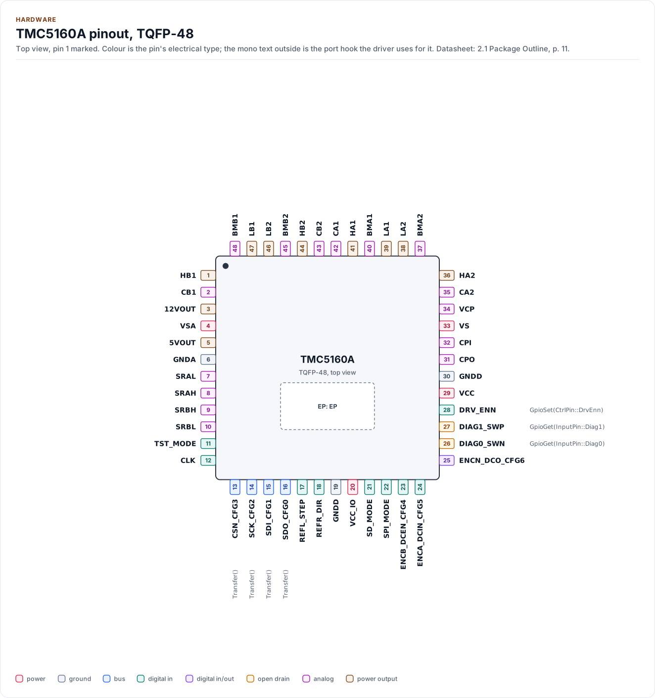
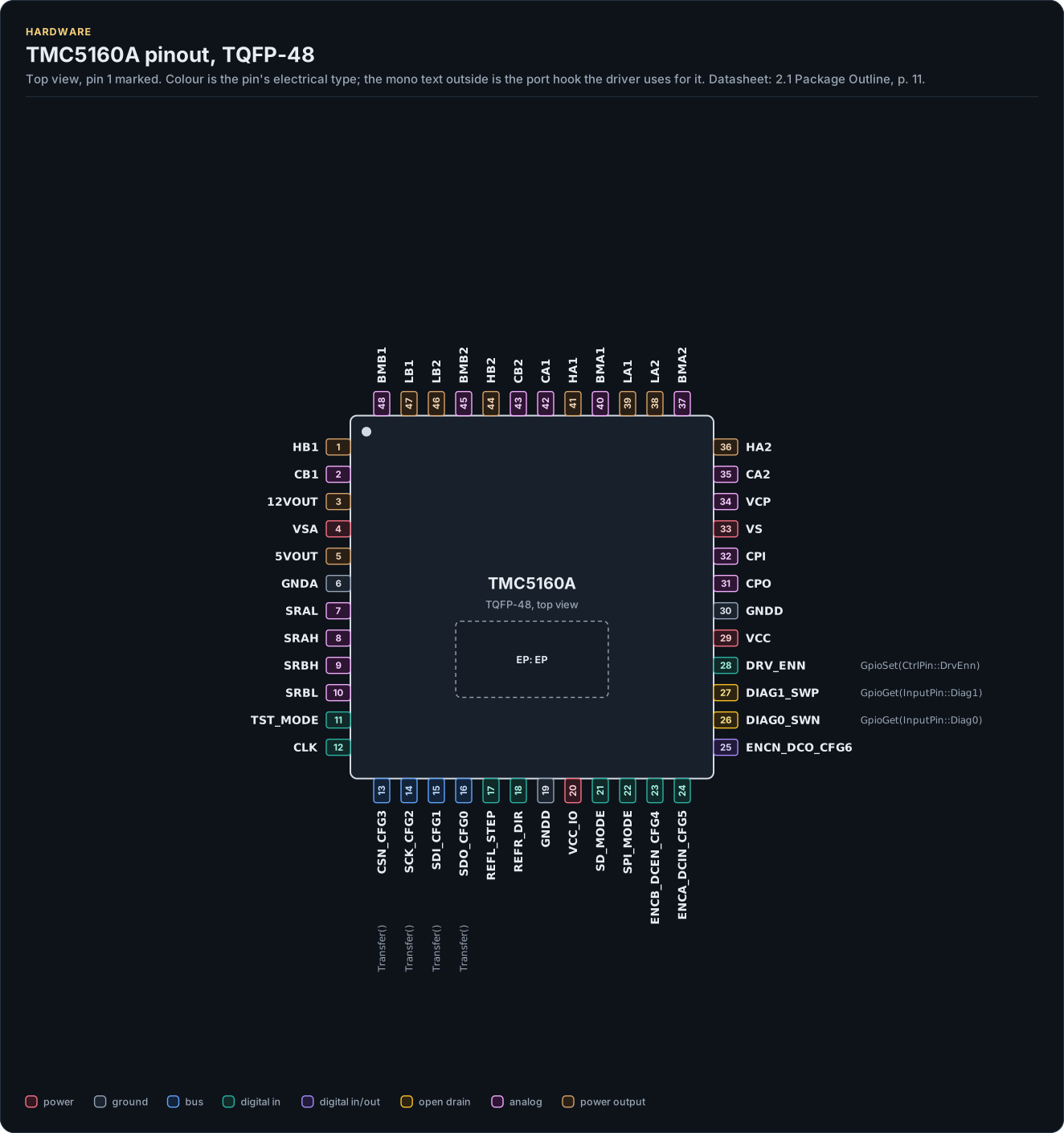
Figure description and sources
The TMC5160A seen from the top, in its TQFP-48 package. Pin 1 is marked by the dot; the numbers run counter-clockwise from it. Each pad is coloured by the pin's electrical type (legend below). Next to it is the pin's name and, in mono, the hook of the driver's port that drives or reads it; a pin without a hook is not used by the driver. The dashed square is the exposed pad.
Drawn from: docs/hardware.yml; inc/tmc5160_spi_interface.hpp; inc/tmc5160_types.hpp; inc/tmc5160_uart_interface.hpp.
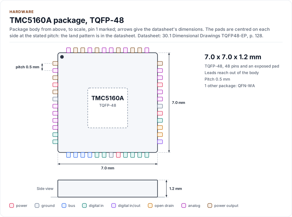
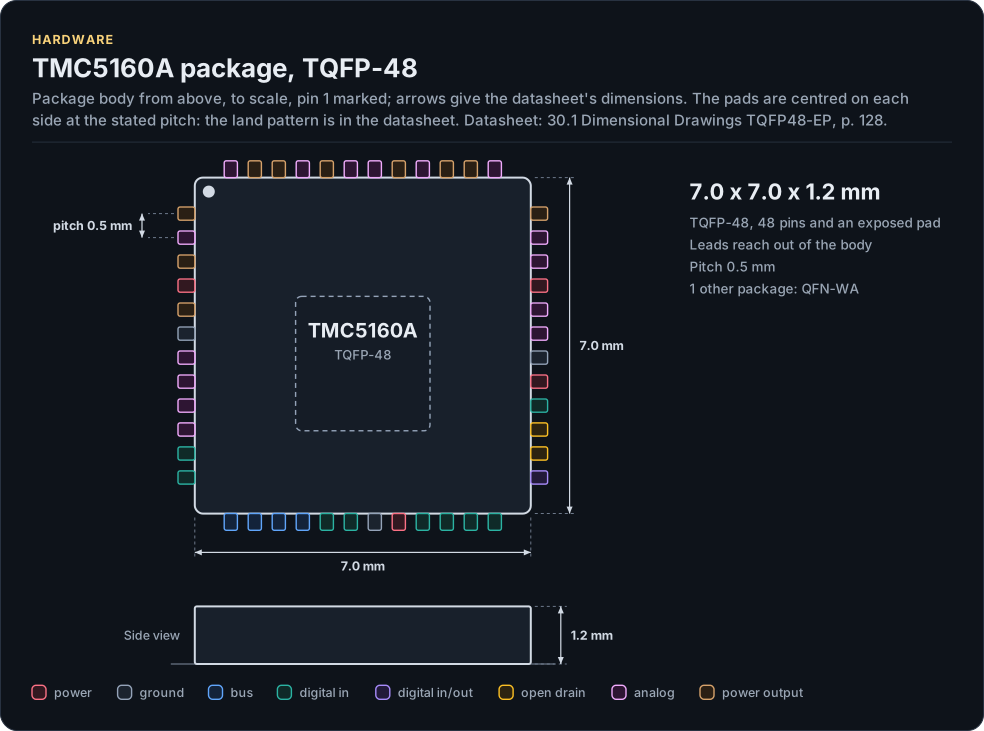
Figure description and sources
The TMC5160A package seen from the top and, when the height is known, from the side, drawn to scale: 7.0 x 7.0 x 1.2 mm. The arrows carry the datasheet's dimensions, the dot marks pin 1 and the pads are numbered counter-clockwise from it, coloured by the pin's electrical type (legend below). Pads sit centred on each side at the stated pitch; the datasheet's land pattern is the reference for a board.
Drawn from: docs/hardware.yml; inc/tmc5160_spi_interface.hpp; inc/tmc5160_types.hpp; inc/tmc5160_uart_interface.hpp.
TQFP-48, 48 pins and an exposed pad (2.1 Package Outline, p. 11).
| Pin | Name | Type (domain) | Function | Driver hook | If unused | Datasheet |
|---|---|---|---|---|---|---|
| 1 | HB1 |
power output (VS) | High-side gate driver output, bridge B1 | - | - | 2.2, p. 12 |
| 2 | CB1 |
analog (VS) | Bootstrap capacitor positive, bridge B1 | - | - | 2.2, p. 12 |
| 3 | 12VOUT |
power output (VSA) | 11.5 V gate regulator output; supplies the low-side drivers | - | - | 2.2, p. 12 |
| 4 | VSA |
power (VSA) | Analog supply for the 11.5 V and 5 V regulators | - | - | 2.2, p. 12 |
| 5 | 5VOUT |
power output (VSA) | 5 V regulator output | - | - | 2.2, p. 12 |
| 6 | GNDA |
ground | Analog ground | - | - | 2.2, p. 12 |
| 7 | SRAL |
analog (VS) | Sense resistor A, ground side | - | - | 2.2, p. 12 |
| 8 | SRAH |
analog (VS) | Sense resistor A, upper side | - | - | 2.2, p. 12 |
| 9 | SRBH |
analog (VS) | Sense resistor B, upper side | - | - | 2.2, p. 12 |
| 10 | SRBL |
analog (VS) | Sense resistor B, ground side | - | - | 2.2, p. 12 |
| 11 | TST_MODE |
digital in (VCC_IO) | Test mode; tie to GND | - | Tie to GND | 2.2, p. 12 |
| 12 | CLK |
digital in (VCC_IO) | Clock input, 4 to 18 MHz; GND selects the internal 12 MHz oscillator | - | Tie to GND | 2.2, p. 12 |
| 13 | CSN_CFG3 |
bus (VCC_IO) | SPI chip select, active low | Transfer() |
- | 2.2, p. 12 |
| 14 | SCK_CFG2 |
bus (VCC_IO) | SPI clock, mode 3, up to 4 MHz on the internal clock | Transfer() |
- | 2.2, p. 12 |
| 15 | SDI_CFG1 |
bus (VCC_IO) | SPI data in; NAI in UART mode | Transfer() |
- | 2.2, p. 12 |
| 16 | SDO_CFG0 |
bus (VCC_IO) | SPI data out, tristate; NAO in UART mode | Transfer() |
- | 2.2, p. 12 |
| 17 | REFL_STEP |
digital in (VCC_IO) | Left reference switch or STEP input | - | Tie to GND | 2.2, p. 12 |
| 18 | REFR_DIR |
digital in (VCC_IO) | Right reference switch or DIR input | - | Tie to GND | 2.2, p. 12 |
| 19 | GNDD |
ground | Digital ground | - | - | 2.2, p. 12 |
| 20 | VCC_IO |
power (VCC_IO) | 3.0 V to 5.25 V I/O supply | - | - | 2.2, p. 12 |
| 21 | SD_MODE |
digital in (VCC_IO) | Low: ramp generator; high: STEP/DIR; both strap pins low: UART | - | Tie to GND | 2.2, p. 12 |
| 22 | SPI_MODE |
digital in (VCC_IO) | High: SPI; low with SD_MODE low: UART; internal pull-down | - | - | 2.2, p. 12 |
| 23 | ENCB_DCEN_CFG4 |
digital in (VCC_IO) | Encoder B, DcStep enable or CFG4; internal pull-down | - | Tie to GND | 2.2, p. 12 |
| 24 | ENCA_DCIN_CFG5 |
digital in (VCC_IO) | Encoder A, DcStep input, emergency stop or CFG5; internal pull-down | - | Tie to GND | 2.2, p. 12 |
| 25 | ENCN_DCO_CFG6 |
digital in/out (VCC_IO) | Encoder N, DcStep ready output or CFG6 | - | Tie to GND | 2.2, p. 12 |
| 26 | DIAG0_SWN |
open drain (VCC_IO) | DIAG0 interrupt or STEP output; SWN of the single wire interface; open drain, 47 k pull-up or less | GpioGet(InputPin::Diag0) |
Leave open | 2.2, p. 12 |
| 27 | DIAG1_SWP |
open drain (VCC_IO) | DIAG1 position compare or DIR output; SWP of the single wire interface; open drain, internal pull-down | GpioGet(InputPin::Diag1) |
Leave open | 2.2, p. 12 |
| 28 | DRV_ENN |
digital in (VCC_IO) | Driver enable, active low | GpioSet(CtrlPin::DrvEnn) |
- | 2.2, p. 12 |
| 29 | VCC |
power (VSA) | 5 V digital supply, from 5VOUT through 2.2 ohm | - | - | 2.2, p. 12 |
| 30 | GNDD |
ground | Digital ground | - | - | 2.2, p. 12 |
| 31 | CPO |
analog (VS) | Charge pump capacitor output | - | - | 2.2, p. 12 |
| 32 | CPI |
analog (VS) | Charge pump capacitor input | - | - | 2.2, p. 12 |
| 33 | VS |
power (VS) | Motor and bridge supply, 10 V to 55 V | - | - | 2.2, p. 12 |
| 34 | VCP |
analog (VS) | Charge pump voltage | - | - | 2.2, p. 12 |
| 35 | CA2 |
analog (VS) | Bootstrap capacitor positive, bridge A2 | - | - | 2.2, p. 12 |
| 36 | HA2 |
power output (VS) | High-side gate driver output, bridge A2 | - | - | 2.2, p. 12 |
| 37 | BMA2 |
analog (VS) | Bridge centre A2 | - | - | 2.2, p. 12 |
| 38 | LA2 |
power output (VSA) | Low-side gate driver output, bridge A2 | - | - | 2.2, p. 12 |
| 39 | LA1 |
power output (VSA) | Low-side gate driver output, bridge A1 | - | - | 2.2, p. 12 |
| 40 | BMA1 |
analog (VS) | Bridge centre A1 | - | - | 2.2, p. 12 |
| 41 | HA1 |
power output (VS) | High-side gate driver output, bridge A1 | - | - | 2.2, p. 12 |
| 42 | CA1 |
analog (VS) | Bootstrap capacitor positive, bridge A1 | - | - | 2.2, p. 12 |
| 43 | CB2 |
analog (VS) | Bootstrap capacitor positive, bridge B2 | - | - | 2.2, p. 12 |
| 44 | HB2 |
power output (VS) | High-side gate driver output, bridge B2 | - | - | 2.2, p. 12 |
| 45 | BMB2 |
analog (VS) | Bridge centre B2 | - | - | 2.2, p. 12 |
| 46 | LB2 |
power output (VSA) | Low-side gate driver output, bridge B2 | - | - | 2.2, p. 12 |
| 47 | LB1 |
power output (VSA) | Low-side gate driver output, bridge B1 | - | - | 2.2, p. 12 |
| 48 | BMB1 |
analog (VS) | Bridge centre B1 | - | - | 2.2, p. 12 |
| EP | EP |
ground | Exposed die pad: GNDD and GNDP, the heat path | - | - | 2.2, p. 12 |
Source of this table and of the chip figures: docs/hardware.yml.
Block diagram
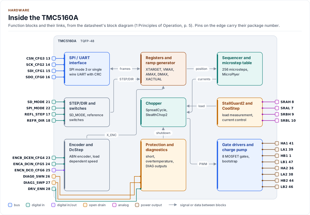
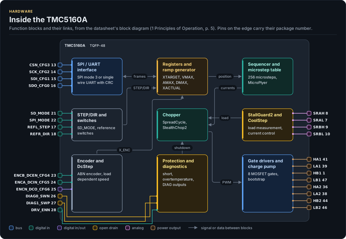
Figure description and sources
The TMC5160A's function blocks inside its outline. Arrows between blocks carry signals or data in the direction they point (both ways where they have two heads). The package pins stand on the left and right edges with their numbers, each wired to the block it reaches.
Drawn from: docs/hardware.yml; inc/tmc5160_spi_interface.hpp; inc/tmc5160_types.hpp; inc/tmc5160_uart_interface.hpp.
Reference circuits
The circuits are drawn from hardware.yml; the part values are the datasheet's (Figure 3.1) except where
marked.
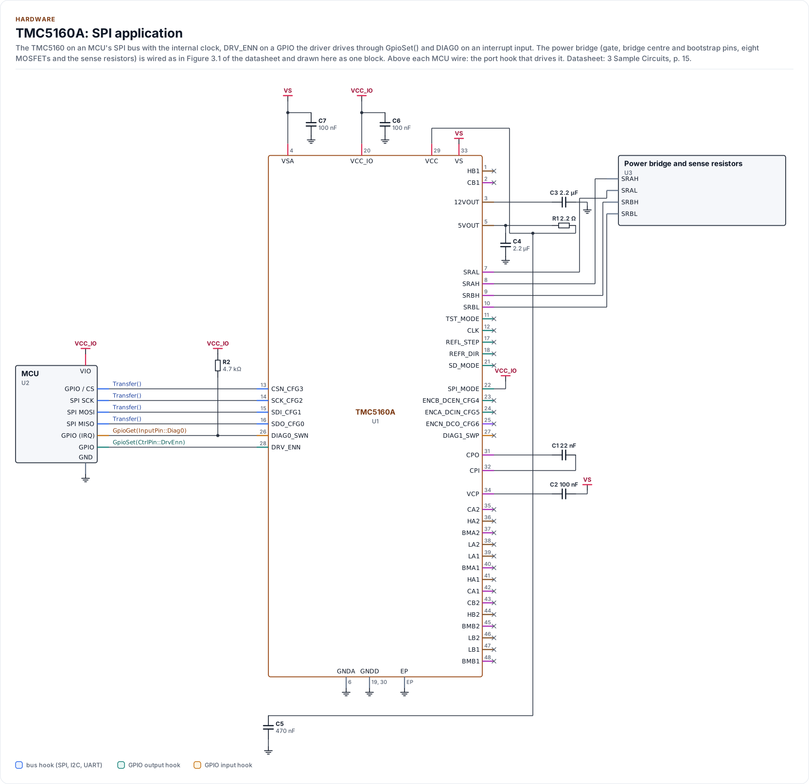
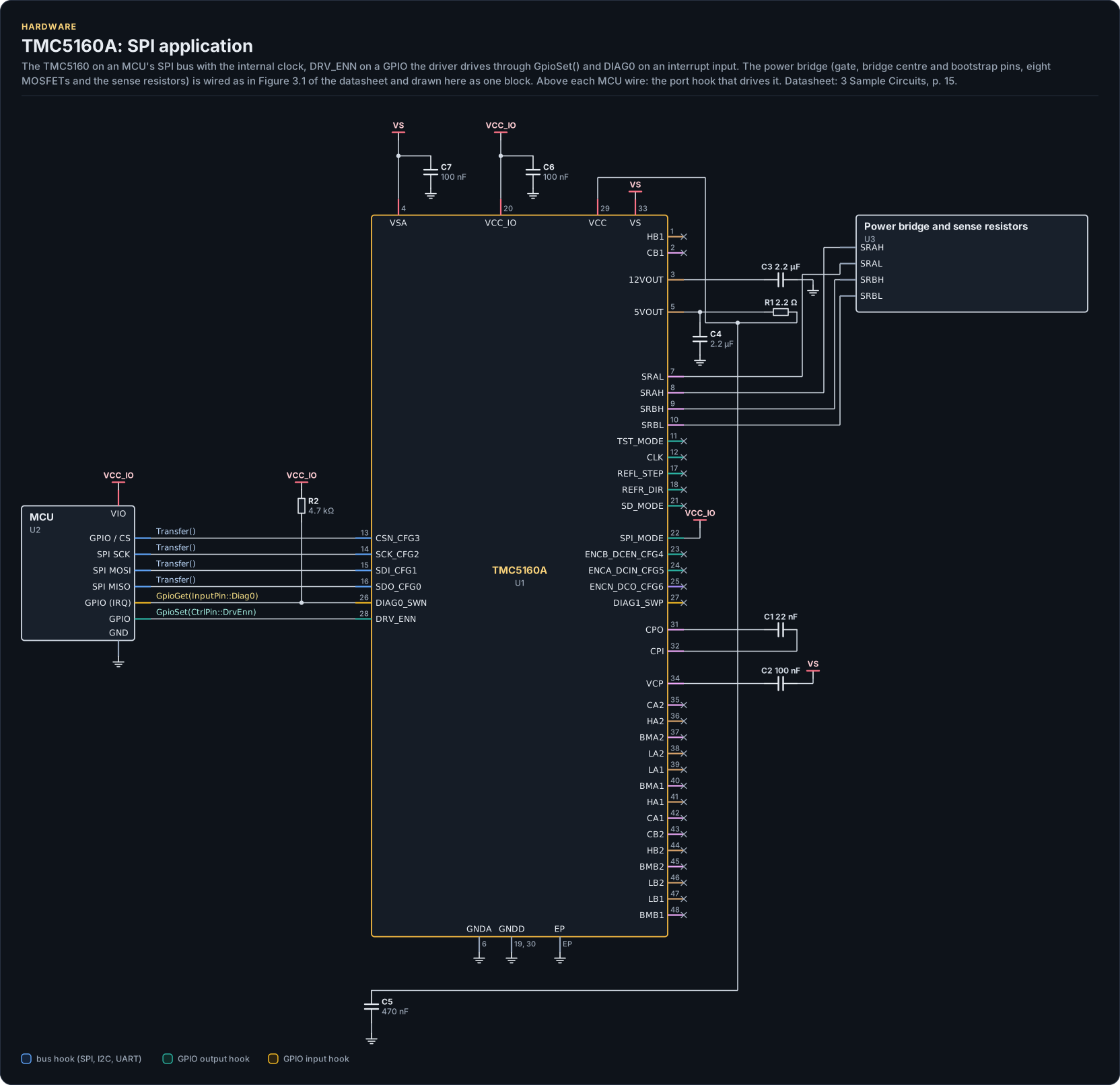
Figure description and sources
A schematic. The MCU is on the left, each of its pins level with the chip pin it connects to; above each wire is the hook of the driver's port that drives or reads it. Supply pins point up to their supply and decoupling, ground pins down. Pins on the right carry the loads and the pins tied to a supply or ground; a cross marks a pin left open. A dot is a junction; wires that cross without a dot are not connected.
Drawn from: docs/hardware.yml; inc/tmc5160_spi_interface.hpp; inc/tmc5160_types.hpp; inc/tmc5160_uart_interface.hpp.
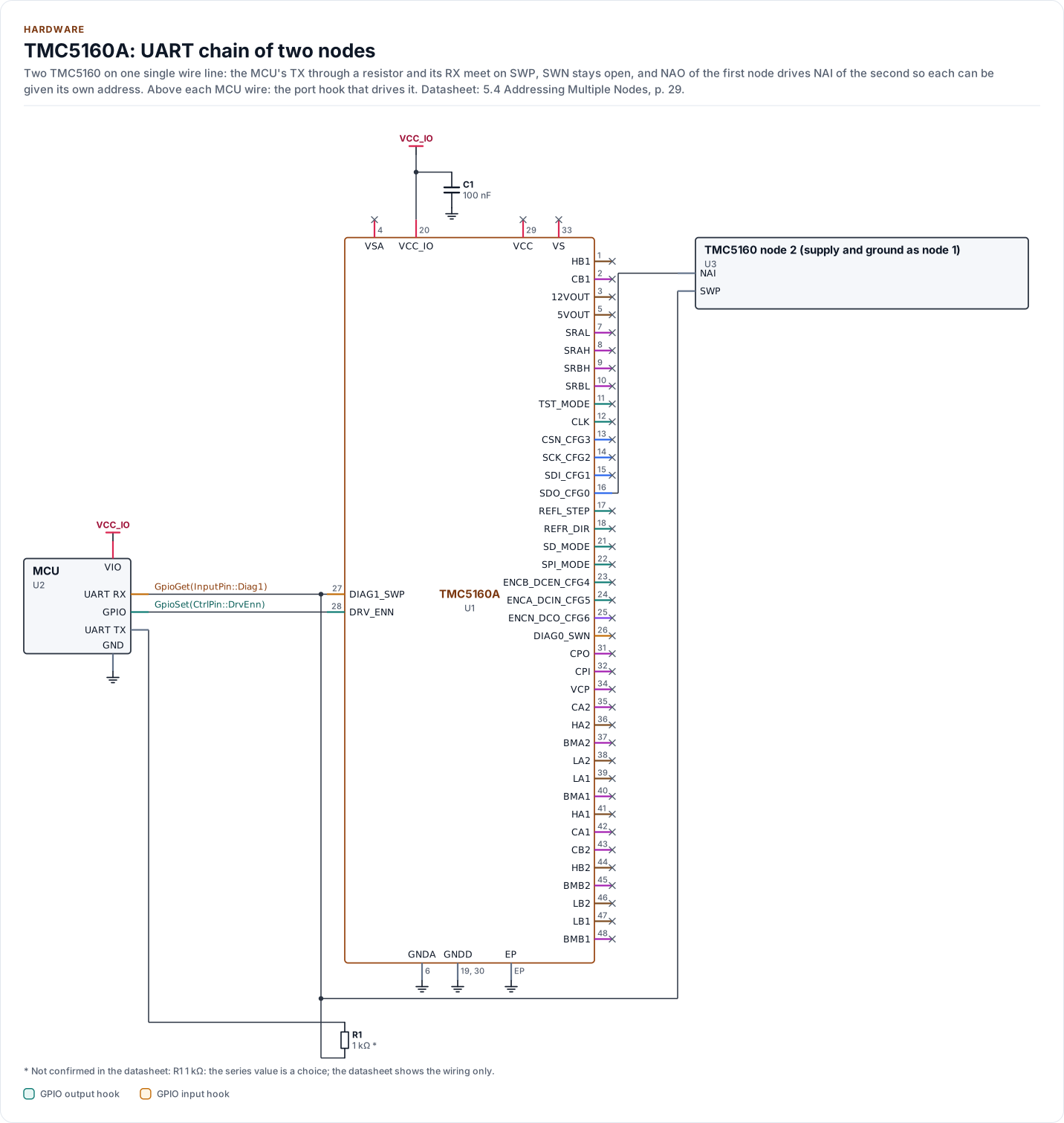
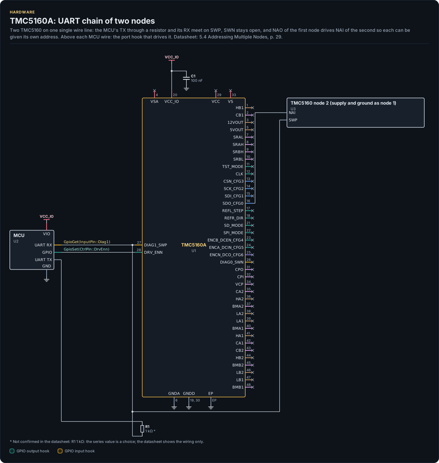
Figure description and sources
A schematic. The MCU is on the left, each of its pins level with the chip pin it connects to; above each wire is the hook of the driver's port that drives or reads it. Supply pins point up to their supply and decoupling, ground pins down. Pins on the right carry the loads and the pins tied to a supply or ground; a cross marks a pin left open. A dot is a junction; wires that cross without a dot are not connected.
Drawn from: docs/hardware.yml; inc/tmc5160_spi_interface.hpp; inc/tmc5160_types.hpp; inc/tmc5160_uart_interface.hpp.
In UART mode the MCU's TX and RX wires to SWP are the Exchange() hook, and DIAG0 and DIAG1 are not available (their
pins are the single wire interface, UART protocol). The figure still labels those pins with their
SPI-mode hooks until the figure tool can give one circuit its own hooks.
SPI application (figure chip-circuit-spi-typical)
| Part | Kind | Value | Connects | Datasheet |
|---|---|---|---|---|
| U2 | MCU | - | VIO: VCC_IO, GND: GND, SCK: SCLK, MOSI: SDI, MISO: SDO, CS: CSN, ENN: DRV_ENN, IRQ: DIAG0 | 3, p. 15 |
| U3 | Power bridge and sense resistors | - | SRAH: SRAH, SRAL: SRAL, SRBH: SRBH, SRBL: SRBL | 3, p. 15 |
| C1 | capacitor | 22 nF | CPI, CPO | 3, p. 15 |
| C2 | capacitor | 100 nF | VS, VCP | 3, p. 15 |
| C3 | capacitor | 2.2 µF | GND, 12VOUT | 3, p. 15 |
| C4 | capacitor | 2.2 µF | GND, 5VOUT | 3, p. 15 |
| C5 | capacitor | 470 nF | GND, VCC | 3, p. 15 |
| C6 | capacitor | 100 nF | VCC_IO, GND | 3, p. 15 |
| C7 | capacitor | 100 nF | VS, GND | 3, p. 15 |
| R1 | resistor | 2.2 Ω | 5VOUT, VCC | 3, p. 15 |
| R2 | resistor | 4.7 kΩ | VCC_IO, DIAG0 | 2.2, p. 12 |
UART chain of two nodes (figure chip-circuit-uart-chain)
| Part | Kind | Value | Connects | Datasheet |
|---|---|---|---|---|
| U2 | MCU | - | VIO: VCC_IO, GND: GND, RX: SWP, TX: TX, ENN: DRV_ENN | 5.4, p. 29 |
| U3 | TMC5160 node 2 (supply and ground as node 1) | - | SWP: SWP, NAI: NAO | 5.4, p. 29 |
| R1 | resistor | 1 kΩ (not confirmed: the series value is a choice; the datasheet shows the wiring only) | SWP, TX | 5.4, p. 29 |
| C1 | capacitor | 100 nF | VCC_IO, GND | 3, p. 15 |
Export a circuit for a schematic or PCB tool: kokeb-docs hardware --kicad-netlist OUT.net --circuit spi-typical.
Operating modes and straps
| Mode | SD_MODE | SPI_MODE | Interface | Driver |
|---|---|---|---|---|
| Motion controller | low | high (SPI) or low (UART) | SPI or UART | Mode::MotionController |
| STEP/DIR with serial configuration | high | high | SPI | Mode::StepDir |
| Standalone STEP/DIR, configured by the CFG pins | high | low | none | not drivable |
EnsureInitialized() reads IOIN and compares the SD_MODE level with Config::mode; a mismatch returns ModeMismatch.
Control pins
The driver drives DRV_ENN, and no other control pin, through the optional GpioSet() hook, with
logical levels: GpioSignal::ACTIVE means "driver enabled", which your port writes as a low level on DRV_ENN. A board
that wires DRV_ENN low permanently leaves the hook out: Enable() then writes TOFF only, and Disable() writes TOFF 0.
Configure the pin with the driver off before it becomes an output.
DIAG0 and DIAG1 are read with GpioGet(). They are open drain by default and need a pull-up of 47 kOhm or less.
Supplies
| Rail | Range | Source |
|---|---|---|
| VS | 10 V to 55 V | Motor and bridge supply (section 28.1, page 120) |
| VSA | 10 V to 50 V | Analog supply for the 11.5 V and 5 V regulators |
| VCC_IO | 3.0 V to 5.25 V | I/O supply, sets the logic levels |
The cover page says 8 V to 60 V; the driver uses the operating range of page 120 (Ambiguities, A50). The slopes of VS at power-on and power-off must stay below 1 V per microsecond, and ripple above 0.5 V endangers the charge pump (pages 15 and 16).
Clock
The internal oscillator runs at about 12 MHz (practical tolerance 4 percent); an external clock of 4 MHz to 18 MHz on CLK
is accepted (10 to 16 MHz advised). Every time, velocity and acceleration value scales with the clock, so declare it in
Config::clock.
Bus settings
| Setting | SPI | UART |
|---|---|---|
| Mode | Mode 3: SCK idle high, sampled on the rising edge | 8N1, LSB first |
| Clock | Up to 4 MHz on the internal clock, fCLK / 2 less a 10 percent margin on an external one |
9000 baud to fCLK / 16, set from the sync nibble |
| Frame | 40 bits, CSN low for the whole frame | 8 bytes write, 4 bytes read request, 8 bytes reply |
| Integrity | none | CRC-8 |
SPI timing (section 4.3, page 25): CSN high time more than 2 tCLK + 10 ns, SCK high and low more than tCLK + 10 ns,
SDI setup and hold 10 ns. The driver does not time the bus: the port's clock sets it.
Timing the driver waits for
| Parameter | Value | Driver |
|---|---|---|
| Interface idle after a UART error | 12 bit times | kUartRecoveryBits |
| StealthChop automatic tuning AT#1 | up to 130 ms | SetStealthChop() waits with bounded DelayUs() calls |
| DRV_ENN switch-off | 3 clock cycles | Disable() |
Reset
A chip reset (undervoltage on VSA, 5VOUT or VCC_IO, or power-up) sets every register to its reset value. VCC is not
monitored (section 25, page 119). After a microcontroller reboot the datasheet asks: TOFF 0, rewrite all registers, stop
the ramp. EnsureInitialized() does exactly that; the driver never relies on the chip's registers surviving.
Reference documents
The datasheet:
TMC5160/TMC5160A datasheet.
Every pin, setting and timing on this page cites a section of it; its revision, its SHA-256 and the sections each page
relies on are in docs/datasheets.yml.
| Document | Revision | Get it |
|---|---|---|
| Datasheet: TMC5160 / TMC5160A Datasheet (Analog Devices (Trinamic) TMC5160A-DS) | 1.18, 2023-03-01 | vendor page |
Written against these revisions; the SHA-256 of each file is in docs/datasheets.yml. Where each part
of the driver is in the datasheet: Datasheet map.
| Also useful | Contents |
|---|---|
inc/tmc5160_registers.hpp |
The register map as the driver uses it, with datasheet section numbers |
| Coverage map | Every pin and rating of the datasheet and where the driver handles it |